 10
10
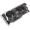
MSI GeForce GTX 465 Twin Frozr II Review
Test Setup »A Closer Look
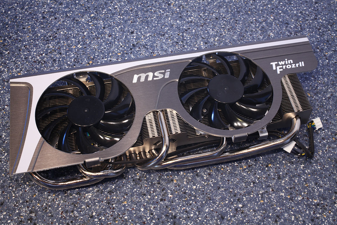


The first step in disassembly is removing the Twin Frozr II cooler, which uses five heatpipes to transport the GPU's heat away from the baseplate to a large number of fins which are cooled by two fans. Once the main heatsink is removed, there is still a metal plate left on the card which cools the memory chips and voltage regulation circuitry.


MSI's heat spreader is made from metal and covers all secondary heat sources.

The last piece that remains on the card is the black stabilizer near the top edge. It is made from metal and serves to protect the card against any bending or warping from the weight of the heatsink (which is not that heavy in my opinion).

The GTX 465 requires two 6-pin PCI-Express power connectors.
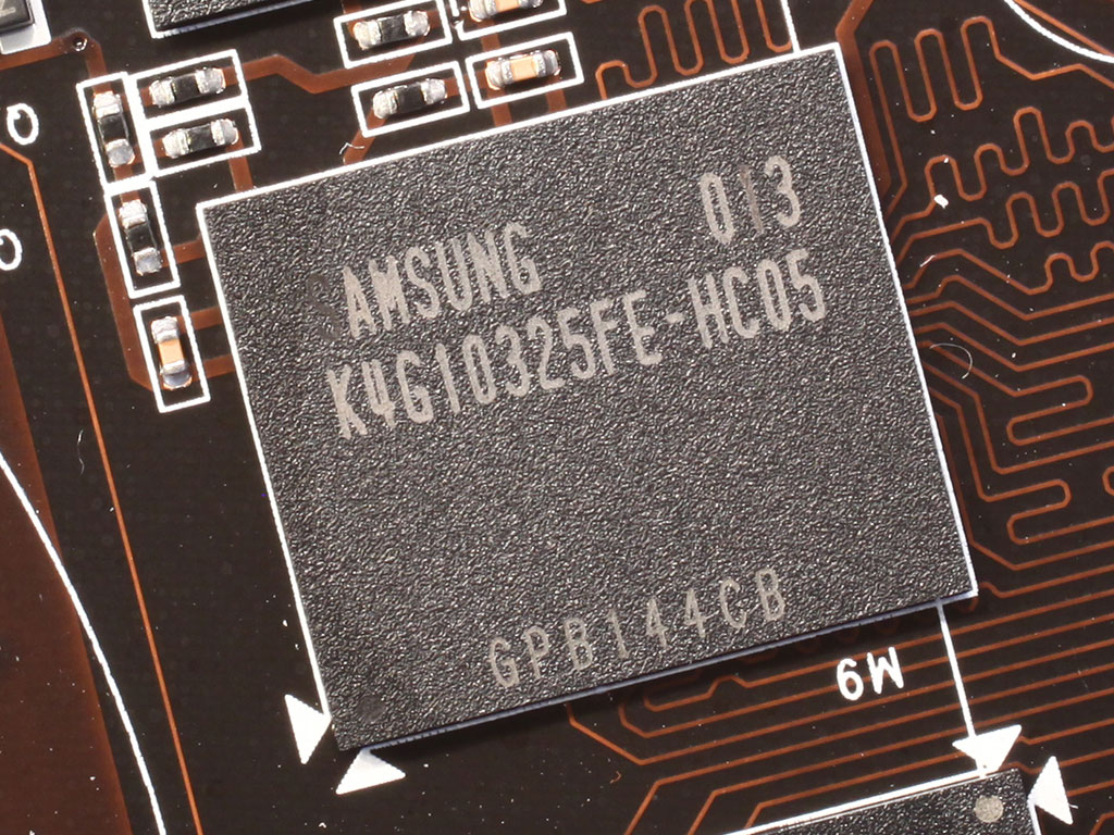
The GDDR5 memory chips are made by Samsung, and carry the model number K4G10325FE-HC05. They are specified to run at 1000 MHz (4000 MHz GDDR5 effective).

OnSemi's NCP5388 is a reasonable priced voltage regulator, unfortunately it does not have I2C voltage control. NVIDIA however exposes an API for voltage changes via VID in their NVAPI, which is used in MSI Afterburner for voltage control.

NVIDIA's GeForce 100 graphics processor is made on a 40 nm process at TSMC Taiwan. It uses approximately 3.2 billion transistors which makes it the most complex GPU built to-date. Please note that the silvery metal surface you see is the heatspreader of the GPU which measures 42.3 x 42.3 mm. The actual GPU die is sitting under the heatspreader, its dimensions are not known. NVIDIA did not communicate a die size measurement to the press.
Apr 23rd, 2024 20:46 EDT
change timezone
Latest GPU Drivers
New Forum Posts
- What's your latest tech purchase? (20319)
- Post your Cinebench 2024 score (449)
- Sexy Mechanical Keyboard Thread (484)
- The TPU UK Clubhouse (24766)
- need help with motherboard/ ram compability certainty (14)
- My computer setup - Request for opinions (12)
- Show us your collections thread!! (282)
- Realtek Modded Audio Driver for Windows 10/11 - Only for HDAUDIO (5687)
- What phone you use as your daily driver? And, a discussion of them. (1454)
- Is there a technical reason that Windows 11 doesn't have built into it battery charge limitation? (37)
Popular Reviews
- Fractal Design Terra Review
- Corsair 2000D Airflow Review
- Thermalright Phantom Spirit 120 EVO Review
- Minisforum EliteMini UM780 XTX (AMD Ryzen 7 7840HS) Review
- ASUS GeForce RTX 4090 STRIX OC Review
- NVIDIA GeForce RTX 4090 Founders Edition Review - Impressive Performance
- ASUS GeForce RTX 4090 Matrix Platinum Review - The RTX 4090 Ti
- MSI GeForce RTX 4090 Gaming X Trio Review
- MSI GeForce RTX 4090 Suprim X Review
- Gigabyte GeForce RTX 4090 Gaming OC Review
Controversial News Posts
- Sony PlayStation 5 Pro Specifications Confirmed, Console Arrives Before Holidays (116)
- NVIDIA Points Intel Raptor Lake CPU Users to Get Help from Intel Amid System Instability Issues (106)
- AMD "Strix Halo" Zen 5 Mobile Processor Pictured: Chiplet-based, Uses 256-bit LPDDR5X (101)
- US Government Wants Nuclear Plants to Offload AI Data Center Expansion (98)
- Windows 10 Security Updates to Cost $61 After 2025, $427 by 2028 (84)
- Developers of Outpost Infinity Siege Recommend Underclocking i9-13900K and i9-14900K for Stability on Machines with RTX 4090 (84)
- TechPowerUp Hiring: Reviewers Wanted for Motherboards, Laptops, Gaming Handhelds and Prebuilt Desktops (74)
- Intel Realizes the Only Way to Save x86 is to Democratize it, Reopens x86 IP Licensing (70)