 29
29
MSI Big Bang Z77 MPower Intel LGA 1155 Review
BIOS Walkthrough »The Board - A Closer Look
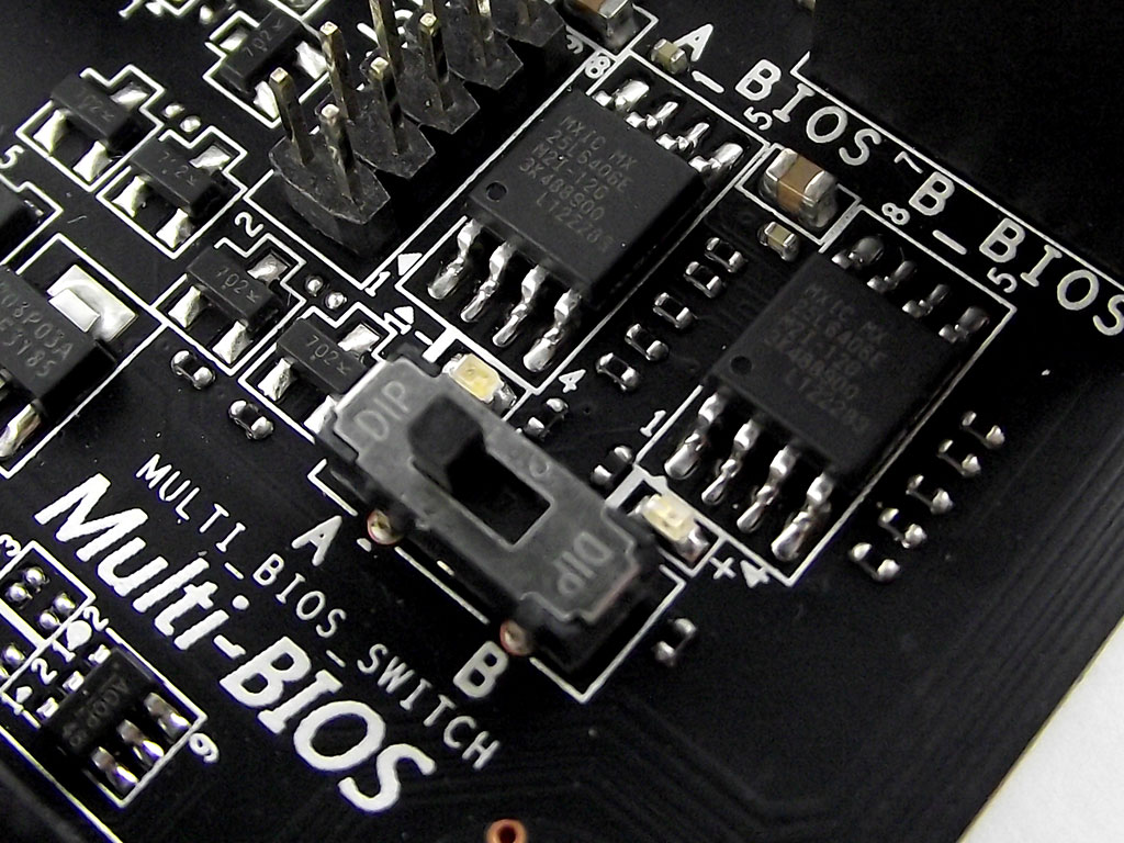

First of all, the MSI Big Bang Z77 Mpower has a rather unique little BIOS hardware implementation, although we have seen the first part on other boards before. The first part is comprised of two actual BIOS chips, and you can choose which one is in use through the switch shown in the first image above. The second part has to do with actually getting into the BIOS, possible through the button in the second image above. How does it work, you say? Just push it, and the next time the board boots, it AUTOMATICALLY enters the BIOS for setting adjustments. Why does it work like that? If you have got Windows 8 installed, it can boot so fast that pressing the "DELETE" key madly will probably never get you into the BIOS, which can be pretty frustrating as an overclocker with Windows 8. MSI has, to fix this issue, added a button, and it completely eliminates that problem, 100% of the time.


To get the board up and running, there are three switches located in the upper right corner of the board. The first two are POWER and RESET, totally common, yet uncommon is the OC Genie button, which allows the board to boot with an overclock by simply pressing that button. The clocks used here are pre-profiled to be compatible with nearly every chip out there and MSI has taken it one step further by allowing you to customize that profile with relative ease inside the BIOS. There is another neat little thing you might want to setup before booting your PC: the V-Check Points, there to keep track of voltages in real time with the aid of a digital multimeter. There are four cables in the box that plug into this header, which you can plug the meter's probes into. They do a pretty decent job of holding onto probes found on most meters, making it far easier to keep the meter plugged in compared to some points of solder other board makers provide. MSI's solution IS, as far as I am concerned, the best way to do this.


MSI knows that an overlocker needs to know what is going on as a PC boots up incase something fails. Right next to the USB 3.0 header is a dual digit LED display that shows POST codes as the board is booting, swapping to show system temperatures after the boot completes. I found a Fintek part, shown in the second image above, responsible for monitoring duties through software in both BIOS and Windows.
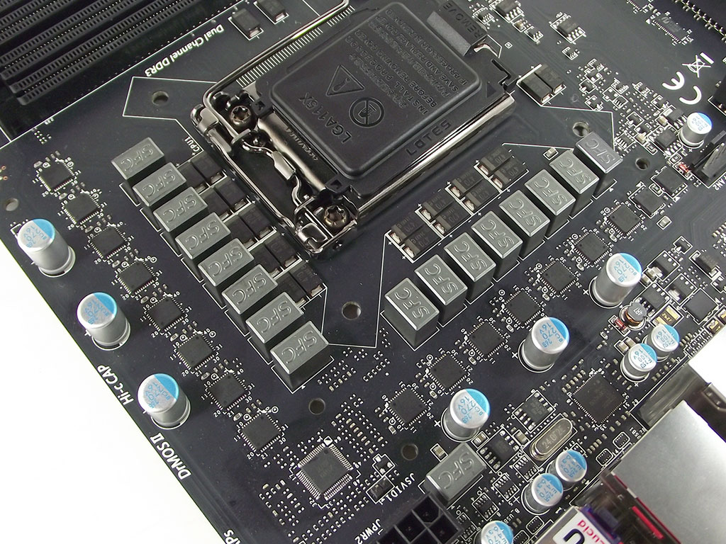

To supply power, MSI uses their standard DRMOS design, part of the "Military Class III" group of components. These parts are both in the CPU VRM and the DIMM VRM, shown in the images above. The CPU VRM has fifteen DRMOS parts, while the DIMM VRM has two. The DIMM VRM does seem to be dual-phase though, while the DRMOS parts on the CPU VRM seem to each power their own phase, rather than one DRMOS for two phases like the DIMM VRM.

To control that, I found a UPI uP1618A, a 6+2 phase controller that is actually pretty popular, although I haven't seen one in a while. That UPI controller is in turn connected to a series of LEDs that indicate which phases are in use. I find it odd that there are so many DRMOS components and just 12 LEDs here. Those other VRMs probably push the iGPU portion of the CPU, and maybe VTT as well. There is also a LED here that indicates if the VRM is overheating, which might not be of use to daily users, but such a LED might prove immensely useful with LN2 or other types of extreme cooling.


The extra rear USB 3.0 ports are provided by an NEC USB 3.0 controller shown in the first image above. The video outputs are driven by a Parade PSB101 TMDS chip shown in the second image above.
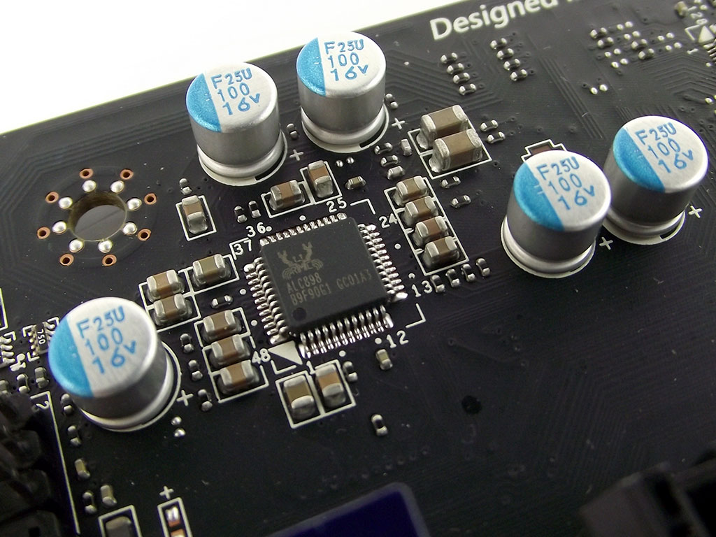
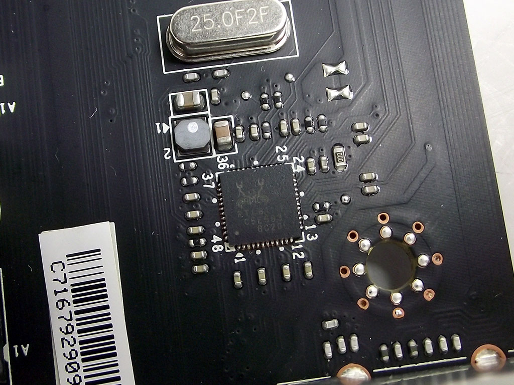
Audio comes via a Realtek ALC898 chipset, a high-end part I've seen many times, but one that has proven quite susceptible to circuit design. It will be interesting to see how well the Z77 MPower does in RightMark Audio Analyzer. The LAN port is also powered by a Realtek part, a very common RTL8111E. I would have preferred an Intel controller here, but the RTL8111E still performs well enough.

Another neat little feature is the ability to remove both the Bluetooth and WiFi dongles that are part of the rear I/O. Those empty slots you see in the first image are the receptacles the dongles sit in, and the second image shows the dongles themselves, with the blue tipped dongle being the Bluetooth controller. Disabling devices when overclocking is just something that is done, and this board does one better by allowing you to remove them altogether!


The PCH cooler is a pretty large radiator covered with a black vanity plate that has a yellow "speed strip" on one side. It's more than overlarge, but great for benchmarking and dual-GPU users, or even those that use triple-slot VGAs, although I am not sure that MSI tests dual-GPU use during their "OC Certified" testing. Another little thing that will be useful to users with multiple GPUs is the PCIe power plug, there to add more power to the PCIe lanes. However, I think MSI made a horrible choice here because many PSUs, like my 750 W Gold-rated Silverstone PSU, only have four PCIe plugs, which also makes PSU choice critical if you really want to clock GPUs to the limit with this motherboard. I can easily imagine that the plug would prove beneficial when you have a couple of MSI Lightning cards installed, so I was rather shocked to see such a plug here because a simple SATA plug would have been more compatible with some PSUs. I cannot ignore that MSI probably thought you only need that plug if you have a good, powerful PSU with more than just four PCIe plugs, but what about triple-card benchmarkers? You would, in that case, need seven plugs from the PSU for PCIe, instead of six.
Apr 23rd, 2024 12:16 EDT
change timezone
Latest GPU Drivers
New Forum Posts
- What's your latest tech purchase? (20299)
- FINAL FANTASY XIV: Dawntrail Official Benchmark (67)
- Is there a technical reason that Windows 11 doesn't have built into it battery charge limitation? (30)
- Asus Crosshair X670E - CPU Package temps (10)
- Core PL1 + GPU PL1 + Ring EDP OTHER (4)
- 5.1 or 7.1 software solutions (1)
- SOYO RX580 2048SP Original Bios (8)
- Unlock the shaders - AMD Radeon RX 560D (323)
- Possible near-future 2024 Arrow Lake build.... (49)
- What are you playing? (20521)
Popular Reviews
- Horizon Forbidden West Performance Benchmark Review - 30 GPUs Tested
- Fractal Design Terra Review
- Corsair 2000D Airflow Review
- Thermalright Phantom Spirit 120 EVO Review
- Minisforum EliteMini UM780 XTX (AMD Ryzen 7 7840HS) Review
- ASUS GeForce RTX 4090 STRIX OC Review
- NVIDIA GeForce RTX 4090 Founders Edition Review - Impressive Performance
- ASUS GeForce RTX 4090 Matrix Platinum Review - The RTX 4090 Ti
- Creative Pebble X Plus Review
- MSI GeForce RTX 4090 Gaming X Trio Review
Controversial News Posts
- Sony PlayStation 5 Pro Specifications Confirmed, Console Arrives Before Holidays (116)
- NVIDIA Points Intel Raptor Lake CPU Users to Get Help from Intel Amid System Instability Issues (105)
- AMD "Strix Halo" Zen 5 Mobile Processor Pictured: Chiplet-based, Uses 256-bit LPDDR5X (101)
- US Government Wants Nuclear Plants to Offload AI Data Center Expansion (98)
- Windows 10 Security Updates to Cost $61 After 2025, $427 by 2028 (84)
- Developers of Outpost Infinity Siege Recommend Underclocking i9-13900K and i9-14900K for Stability on Machines with RTX 4090 (82)
- TechPowerUp Hiring: Reviewers Wanted for Motherboards, Laptops, Gaming Handhelds and Prebuilt Desktops (74)
- Intel Realizes the Only Way to Save x86 is to Democratize it, Reopens x86 IP Licensing (70)