 344
344
NVIDIA GeForce GTX 680 Kepler 2 GB Review
Test Setup »A Closer Look

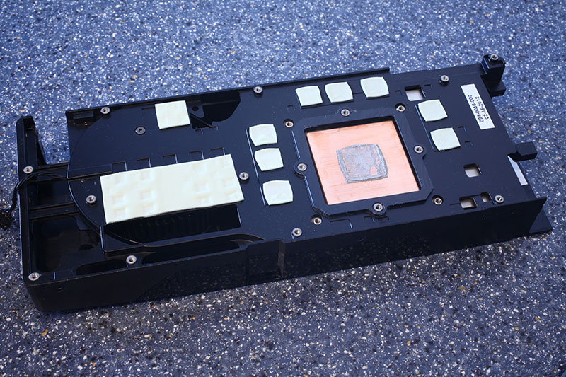
NVIDIA's heatsink may look simple on the outside, but as the second picture shows it is an elaborate construction that cools GPU, memory and voltage regulation circuitry at the same time.
One thing that I noticed is that the cooler emits a strong smell of solvents when the card is loaded. This is not the typical "new graphics card" smell, but something more like glue. Even after a week of testing, it has not completely gone away, but gotten much less intense.

The card requires two 6-pin PCI-Express power connectors. This configuration is good for up to 225 W of power draw. NVIDIA claims that this stacked power connector configuration is better, but I personally don't like it. It makes plugging cables in and out more difficult and the bottom connector is rotated by 180° from what we are used to.
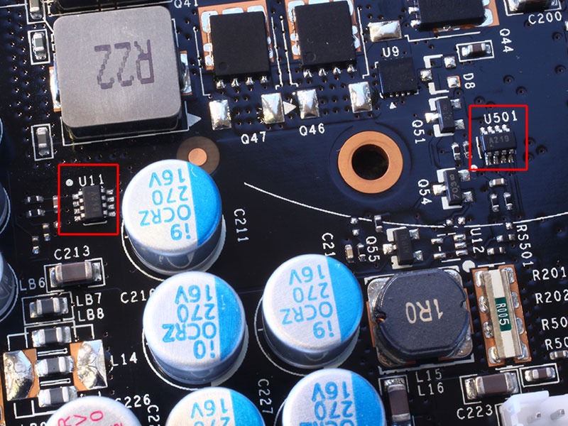
Three of these INA219 power monitor chips are located on the board (the third one is on the other side). These provide voltage, current and power monitoring for 12V PCI-E power, and both 6-pin power connectors. They are used to provide realtime power consumption numbers to the driver, which will then use that info to enable dynamic overclocking and ensure the board does not go above its rated TDP.

NVIDIA has chosen to use a Richtek RT8802A voltage controller on their card. This is a fairly simple controller which does not offer any monitoring features or software voltage control. Voltages are controlled via VID pins that are directly connected to the GPU.
Also note how the chip sits on its own little PCB, which could hint that this is a modular design that will accept different, more advanced controllers, too.

The GDDR5 memory chips are made by Hynix, and carry the model number H5GQ2H24MFR-R0C. They are specified to run at 1500 MHz (6000 MHz GDDR5 effective).

NVIDIA's new GK104 graphics processor introduces the company's brand-new Kepler architecture. It is NVIDIA's first chip to be produced on a 28 nanometer process, at TSMC Taiwan. The transistor count is 3.54 billion.
Apr 19th, 2024 15:28 EDT
change timezone
Latest GPU Drivers
New Forum Posts
- Will a RTX 4070 TI super bottleneck a Ryzen 9 7950X3D? (39)
- [WIN11] 5700x3d Security processor Attestation: Not supported? (3)
- Is it possible to use Linux without the Terminal/command line? (27)
- Linus watercools (45)
- Which air cooler for a ryzen 9 5900x (160)
- Which terminal emulator do you use the most? (9)
- I9 13890HX undervolting Suggestions (2)
- Whats your favourite Linux Distro? (52)
- DDR5 RAM Speeds and the future (50)
- What can be changed in a VBIOS file? (PCI vendor etc) (4)
Popular Reviews
- Horizon Forbidden West Performance Benchmark Review - 30 GPUs Tested
- PowerColor Radeon RX 7900 GRE Hellhound Review
- Fractal Design Terra Review
- Corsair 2000D Airflow Review
- Thermalright Phantom Spirit 120 EVO Review
- Minisforum EliteMini UM780 XTX (AMD Ryzen 7 7840HS) Review
- Creative Pebble X Plus Review
- FiiO KB3 HiFi Mechanical Keyboard Review - Integrated DAC/Amp!
- ASUS GeForce RTX 4090 STRIX OC Review
- NVIDIA GeForce RTX 4090 Founders Edition Review - Impressive Performance
Controversial News Posts
- Sony PlayStation 5 Pro Specifications Confirmed, Console Arrives Before Holidays (110)
- NVIDIA Points Intel Raptor Lake CPU Users to Get Help from Intel Amid System Instability Issues (102)
- US Government Wants Nuclear Plants to Offload AI Data Center Expansion (98)
- Windows 10 Security Updates to Cost $61 After 2025, $427 by 2028 (82)
- Developers of Outpost Infinity Siege Recommend Underclocking i9-13900K and i9-14900K for Stability on Machines with RTX 4090 (82)
- AMD "Strix Halo" Zen 5 Mobile Processor Pictured: Chiplet-based, Uses 256-bit LPDDR5X (76)
- TechPowerUp Hiring: Reviewers Wanted for Motherboards, Laptops, Gaming Handhelds and Prebuilt Desktops (72)
- Intel Realizes the Only Way to Save x86 is to Democratize it, Reopens x86 IP Licensing (70)