News Posts matching #Samsung

Return to Keyword Browsing

Manufacturers Anticipate Completion of NVIDIA's HBM3e Verification by 1Q24; HBM4 Expected to Launch in 2026

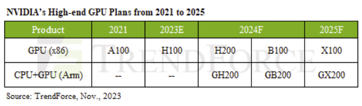
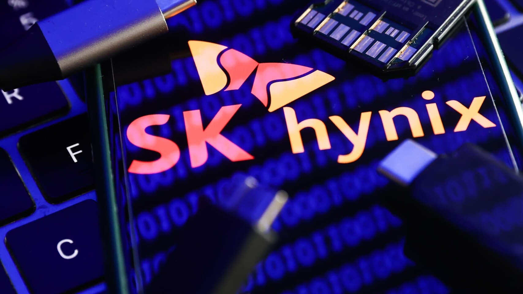
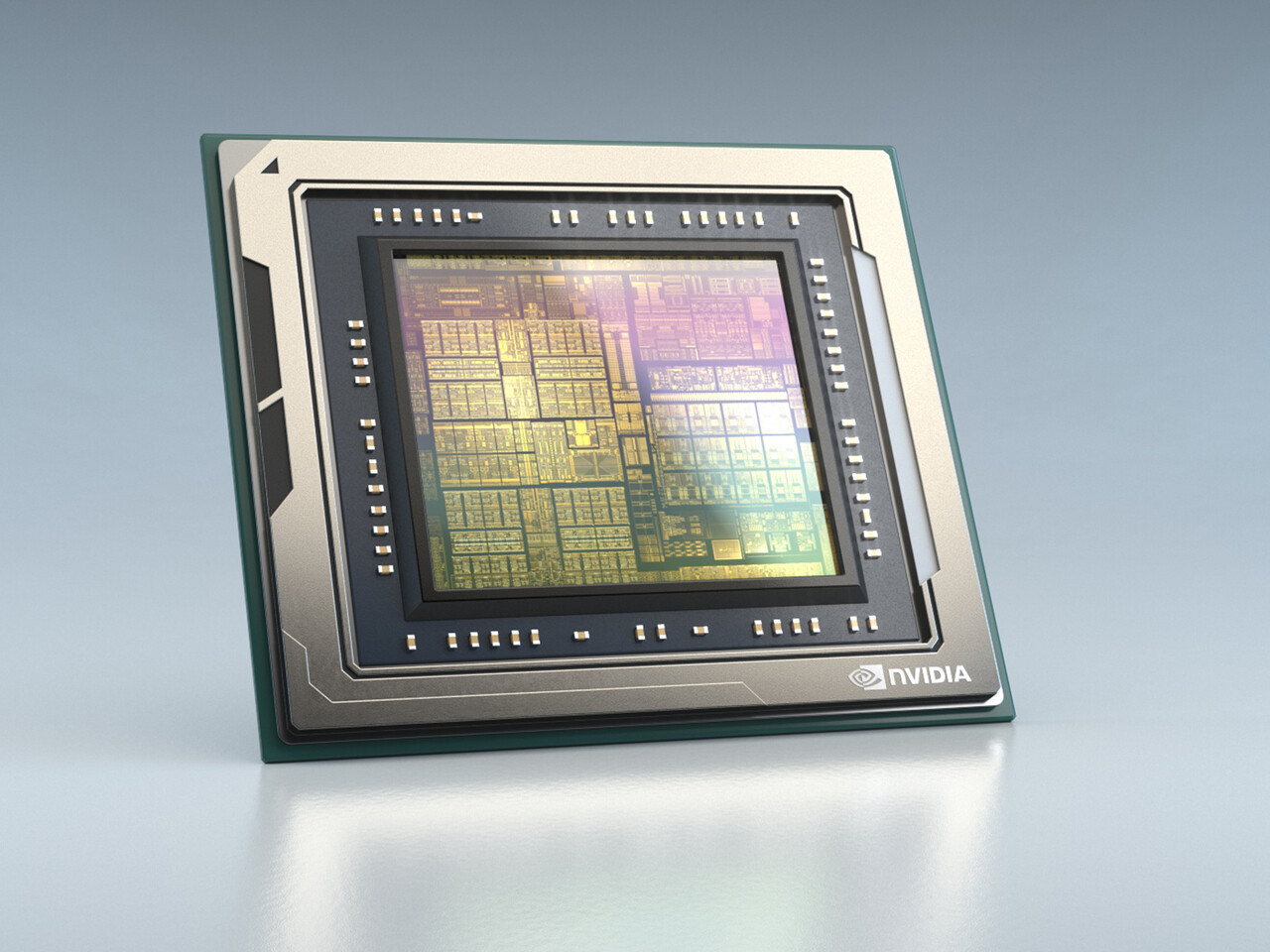
TrendForce's latest research into the HBM market indicates that NVIDIA plans to diversify its HBM suppliers for more robust and efficient supply chain management. Samsung's HBM3 (24 GB) is anticipated to complete verification with NVIDIA by December this year. The progress of HBM3e, as outlined in the timeline below, shows that Micron provided its 8hi (24 GB) samples to NVIDIA by the end of July, SK hynix in mid-August, and Samsung in early October.

Given the intricacy of the HBM verification process—estimated to take two quarters—TrendForce expects that some manufacturers might learn preliminary HBM3e results by the end of 2023. However, it's generally anticipated that major manufacturers will have definite results by 1Q24. Notably, the outcomes will influence NVIDIA's procurement decisions for 2024, as final evaluations are still underway.

NVIDIA Experiences Strong Cloud AI Demand but Faces Challenges in China, with High-End AI Server Shipments Expected to Be Below 4% in 2024

NVIDIA's most recent FY3Q24 financial reports reveal record-high revenue coming from its data center segment, driven by escalating demand for AI servers from major North American CSPs. However, TrendForce points out that recent US government sanctions targeting China have impacted NVIDIA's business in the region. Despite strong shipments of NVIDIA's high-end GPUs—and the rapid introduction of compliant products such as the H20, L20, and L2—Chinese cloud operators are still in the testing phase, making substantial revenue contributions to NVIDIA unlikely in Q4. Gradual shipments increases are expected from the first quarter of 2024.

The US ban continues to influence China's foundry market as Chinese CSPs' high-end AI server shipments potentially drop below 4% next year
TrendForce reports that North American CSPs like Microsoft, Google, and AWS will remain key drivers of high-end AI servers (including those with NVIDIA, AMD, or other high-end ASIC chips) from 2023 to 2024. Their estimated shipments are expected to be 24%, 18.6%, and 16.3%, respectively, for 2024. Chinese CSPs such as ByteDance, Baidu, Alibaba, and Tencent (BBAT) are projected to have a combined shipment share of approximately 6.3% in 2023. However, this could decrease to less than 4% in 2024, considering the current and potential future impacts of the ban.

Samsung Galaxy Book 4 Series Powered by Next Gen Core, Arc and RTX 40-series Graphics

The full specifications of Samsung's upcoming Galaxy Book 4 line of ultra portable notebooks, have been leaked to the web by Windows Report. The star attraction with these notebooks are the next-generation Intel Core processors (possibly "Meteor Lake"), combined with LPDDR4X, LPDDR5, or LPDDR5X memory, the company's latest NVMe SSD storage, and innovative new display panels. There are as many as 5 main models based on form-factor and market segment, and their sub-variants based on memory or storage sizes. The series begins simply with the Galaxy Book 4, with a conventional thickness body and 15.6-inch screen size. This notebook has a conventional IPS panel with anti-glare treatment, and Full HD (1920 x 1080) resolution. At the heart is a Core 5-120U processor that boosts up to 5.00 GHz, and has 12 MB of L3 cache. The notebook uses the iGPU of this processor, and combines it with 8 GB of LPDDR4X memory. There are two M.2 NVMe slots, one of which has a pre-installed 512 GB SSD. Comms include Wi-Fi 6 and Bluetooth 5.1.

The Galaxy Book 4 360 is a step up, and is a convertible. This looks similar to the Galaxy Book 4, but with a screen hingle that turns it into a tablet. The 15.6-inch display now gets an AMOLED touchscreen with Full HD resolution. While the processor is the same Core 5-120U, the 8 GB of memory is faster LPDDR5. You still get two M.2 NVMe slots, one of which has a 256 GB SSD. The communications are a step up, too, with Wi-Fi 6E and Bluetooth 5.3. Both the Galaxy Book 4 and Galaxy Book 4 360 should be priced around the $1,000-mark.

Samsung Unveils New Portable SSD T5 EVO

Samsung Electronics, a world leader in advanced semiconductor technology, today unveiled the T5 EVO, a lightweight portable Solid-State Drive (SSD) that provides up to 8 terabytes (TB) of capacity, which is the largest capacity size currently offered by portable SSDs available on the market. Along with its capacity, the T5 EVO delivers ultra-fast speeds in a compact, durable design as a cutting-edge, versatile SSD solution.

"For consumers who are looking for substitutes for traditional hard disk drives (HDDs), the T5 EVO - offering the largest-available capacity along with speed and durability in a compact design that fits in the palm of your hand - is an innovative, new external storage option," said Hangu Sohn, Vice President of the Memory Brand Product Biz Team at Samsung Electronics. "The T5 EVO is built to fulfill the needs of a wide range of consumers with diverse lifestyles. Its capacity of up to 8 TB, fast speeds, compact design and data protection from external shocks are well-suited for users who want to store and access data anywhere, anytime."

AMD FidelityFX Super Resolution Could Come to Samsung and Qualcomm SoCs

AMD FidelityFX Super Resolution (FSR) is an open-source resolution upscaling technology that takes lower-resolution input and uses super-resolution temporal upscaling technology, frame generation using AMD Fluid Motion Frames (AFMF) technology, and built-in latency reduction technology to provide greater-resolution output images from lower-resolution settings. While the technology is open-source, it battles in market share with NVIDIA and the company's Deep Learning Super Sampling (DLSS). However, in the mobile space, there hasn't been much talk about implementing upscaling technology up until now. According to a popular leaker @Tech_Reve on X/Twitter, we have information that AMD is collaborating with Samsung and Qualcomm to standardize on upscaling technology implementations in mobile SoCs.

Not only does the leak imply that the AMD FSR technology will be used in Samsung's upcoming Exynos SoC, but some AMD ray tracing will be present as well. The leaker has mentioned Qualcomm, which means that future iterations of Snapdragon are up to adopt the FSR algorithmic approach to resolution upscaling. We will see how and when, but with mobile games growing in size and demand, FSR could come in handy to provide mobile gamers with a better experience. Primarily, this targets Android devices, which Qualcomm supplies, where Apple's iPhone recently announced MetalFX Upscaling technology with an A17 Pro chip.

Samsung Said to be Increasing NAND Pricing by 20% Per Quarter

If you've been putting off purchasing that shiny new SSD, you might want to consider doing it before the end of the year, especially if you've been eyeing a model from Samsung, as the company will reportedly be increasing the pricing of its NAND flash starting now. NAND flash might have hit rock bottom, with all major manufacturers except possibly YMTC having cut production to try to push up pricing, but so far, nothing appears to have worked. Despite this, reports coming out of Taiwan's UDN News via TrendForce are suggesting that Samsung is getting ready to hike the price of its NAND flash products by 20 percent per quarter until the middle of 2024.

Admittedly this only gives Samsung about two and a half quarters to increase the pricing, but that's potentially three increases of 20 percent per increase. Samsung has reportedly already increased its NAND wafer prices by 10 to 20 percent this quarter, which according to TrendForce has had a knock on effect on enterprise SSD pricing, which has increased by five to 10 percent already. TrendForce is forecasting a consumer SSD price increase of eight to 13 percent before the end of the year, which might not seem like much, but if the pricing increases for another couple of quarters, we could be looking at 30 to 40 percent more expensive SSDs in the not too distant future. As such, it's going to be worth keeping an eye on SSD pricing, as it's likely that Samsung's competitors will follow suit and increase their NAND pricing as well, which will affect the broader market.

Samsung Electronics Announces Third Quarter 2023 Results

Samsung Electronics today reported financial results for the third quarter ended September 30, 2023. Total consolidated revenue was KRW 67.40 trillion, a 12% increase from the previous quarter, mainly due to new smartphone releases and higher sales of premium display products. Operating profit rose sequentially to KRW 2.43 trillion based on strong sales of flagship models in mobile and strong demand for displays, as losses at the Device Solutions (DS) Division narrowed.

The Memory Business reduced losses sequentially as sales of high valued-added products and average selling prices somewhat increased. Earnings in system semiconductors were impacted by a delay in demand recovery for major applications, but the Foundry Business posted a new quarterly high for new backlog from design wins. The mobile panel business reported a significant increase in earnings on the back of new flagship model releases by major customers, while the large panel business narrowed losses in the quarter. The Device eXperience (DX) Division achieved solid results due to robust sales of premium smartphones and TVs. Revenue at the Networks Business declined in major overseas markets as mobile operators scaled back investments.

Kioxia and Western Digital Merger Stops Due to SK Hynix Opposition

According to sources close to Nikkei, the merger discussions between Western Digital and Kioxia has been terminated. Western Digital notified Kioxia about scrapping the possible transaction, citing the failure to obtain approval from SK Hynix, a significant shareholder of Kioxia, and disagreements over merger terms with Bain Capital, Kioxia's main shareholder. Western Digital and Kioxia, holding the fourth and second positions in the global NAND flash memory market, respectively, planned to join their NAND operations under one roof to create the world's largest maker of NAND memory and potentially enhance their competitive standing and profitability.

The merger was seen as a strategic move to rival Samsung's market dominance by leveraging the companies' combined resources and capabilities, and the plan was to happen as soon as the end of this month. However, the merger faced substantial opposition from SK Hynix, the world's third-largest NAND supplier with a 17.8% market share. Having invested more than $2.6 billion in a consortium led by Bain Capital that previously acquired Kioxia in 2018, SK Hynix expressed concerns that the proposed merger would adversely impact its market position and future collaboration opportunities with Kioxia. This opposition proved to be a pivotal obstacle, preventing the realization of the merger.

Samsung Announces the Galaxy Tab A9 and Galaxy Tab A9+

Samsung Electronics today announced its new Galaxy Tab A9 series, delivering Samsung Galaxy's awesome tablet experiences at great value. Available in two sizes, the series combines immersive video and audio with hyper-fast connectivity—supporting everyday entertainment and productivity needs in a portable package. The Galaxy Tab A9 and Galaxy Tab A9+ exemplify the Galaxy connected ecosystem, offering a continuous experience across multiple devices, as well as innovative ways for users and their loved ones to safely navigate the digital realm.

"We believe everyone deserves the opportunity to experience the latest innovations in tablet technology," said TM Roh, President and Head of Samsung Electronics' Mobile eXperience Business. "With the latest Galaxy Tab A series release, we're making it easier than ever for all to enjoy great entertainment and productive multitasking across the entire Galaxy ecosystem."

Kioxia and Western Digital Could Announce Merger This Month

According to Kyodo News, Japanese chip manufacturer Kioxia and its U.S. counterpart Western Digital are reportedly on the verge of finalizing a merger agreement, aiming to create the world's largest producer of memory chips. The merger plan involves establishing a holding company to consolidate their operations for producing NAND flash memory chips, with the announcement reportedly coming this month. The merged entity is expected to be listed on the Nasdaq stock exchange in the United States. As the global semiconductor market contends with competitive pressures and fluctuating demand, the merger is seen as a strategic move to enhance the combined market position of both companies.

Western Digital shareholders are anticipated to hold a majority stake in the new entity, with Kioxia's shareholders, including Toshiba Corporation, owning the remaining stake. The move is poised to give the newly formed company a combined market share of 35.4 percent in NAND memory chips as of March, surpassing South Korea's Samsung, the current leader, with 34.3 percent. However, the merger's ultimate approval hinges on regulators' decisions, including those in China, as semiconductors have become increasingly integral to global economic security. Major Japanese banks, including MUFG Bank and the state-backed Development Bank of Japan, are contemplating loans of up to approximately 1.9 trillion yen (about $12.7 billion) to facilitate the merger.

Samsung Electronics Holds Memory Tech Day 2023 Unveiling New Innovations To Lead the Hyperscale AI Era

Samsung Electronics Co., Ltd., a world leader in advanced memory technology, today held its annual Memory Tech Day, showcasing industry-first innovations and new memory products to accelerate technological advancements across future applications—including the cloud, edge devices and automotive vehicles.

Attended by about 600 customers, partners and industry experts, the event served as a platform for Samsung executives to expand on the company's vision for "Memory Reimagined," covering long-term plans to continue its memory technology leadership, outlook on market trends and sustainability goals. The company also presented new product innovations such as the HBM3E Shinebolt, LPDDR5X CAMM2 and Detachable AutoSSD.

Samsung V-NAND with 300+ Layers is Coming in 2024, Notes Company Executive

Jung-Bae Lee, President and Head of Memory Business of Samsung Electronics, the world's largest NAND memory supplier, has noted in the blog post that Samsung plans to develop its 9th Generation V-NAND memory with over 300 layers, aiming for mass production in 2024. Samsung's V-NAND uses a double-stack structure and is expected to have more active layers than its competitors' 3D NAND memory, such as SK Hynix's forthcoming 321-layer memory. The increase in layers allows Samsung to enhance storage density and performance in its future 3D NAND devices, focusing on input/output (I/O) speed. While the specific performance details of Samsung's 9th Generation V-NAND remain undisclosed, the memory is expected to be used in next-generation PCIe SSDs with the PCIe 5.0 standard.

Jung-Bae Lee has noted: "New structural and material innovations will be critical in the upcoming era of sub-10-nanometer (nm) DRAM and 1,000-layer vertical V-NAND. As such, we are developing 3D stacked structures and new materials for DRAM while increasing layer count, decreasing height, and minimizing cell interference for V-NAND." The 9th installment of V-NAND, scheduled for 2024, is utilizing 11 nm-class DRAM. Additionally, the blog post reassures the commitment to CXL Memory Modules (CMM), which will enable the composable infrastructure of next-generation systems, especially with high-capacity SSDs powered by V-NAND.

Samsung Notes: HBM4 Memory is Coming in 2025 with New Assembly and Bonding Technology

According to the editorial blog post published on the Samsung blog by SangJoon Hwang, Executive Vice President and Head of the DRAM Product & Technology Team at Samsung Electronics, we have information that High-Bandwidth Memory 4 (HBM4) is coming in 2025. In the recent timeline of HBM development, we saw the first appearance of HBM memory in 2015 with the AMD Radeon R9 Fury X. The second-generation HBM2 appeared with NVIDIA Tesla P100 in 2016, and the third-generation HBM3 saw the light of the day with NVIDIA Hopper GH100 GPU in 2022. Currently, Samsung has developed 9.8 Gbps HBM3E memory, which will start sampling to customers soon.

However, Samsung is more ambitious with development timelines this time, and the company expects to announce HBM4 in 2025, possibly with commercial products in the same calendar year. Interestingly, the HBM4 memory will have some technology optimized for high thermal properties, such as non-conductive film (NCF) assembly and hybrid copper bonding (HCB). The NCF is a polymer layer that enhances the stability of micro bumps and TSVs in the chip, so memory solder bump dies are protected from shock. Hybrid copper bonding is an advanced semiconductor packaging method that creates direct copper-to-copper connections between semiconductor components, enabling high-density, 3D-like packaging. It offers high I/O density, enhanced bandwidth, and improved power efficiency. It uses a copper layer as a conductor and oxide insulator instead of regular micro bumps to increase the connection density needed for HBM-like structures.

OLED Monitor Shipments Predicted to Soar by 323% in 2023; 2024 Shipments Expected to Surpass One Million Units

TrendForce reports that the ever-expanding dimensions of OLED products, combined with the ambitious plans of several top-tier brands, mean that 2023 could see OLED monitor shipments hitting a staggering 508,000 units—an astronomical YoY surge of 323%. Come 2024, the OLED landscape will be richer with more diverse product sizes and specifications. Add to that the debut of the 27-inch and 31.5-inch OLED panels by two leading Korean panel makers, and the arena is set for a showdown. Such dynamics are predicted to catapult OLED monitor shipments past the coveted one million unit threshold.

In terms of market share, Samsung is on track for a spirited push in OLED monitor shipments in 2H23, potentially capturing a market share of 27%—echoing LGE's performance. Not to be left behind, Dell is ardently pushing its 34-inch offering, hoping to clinch a market presence above 20%. Meanwhile, ASUS, having strategically positioned itself in the OLED monitor sector recently, is eyeing a market share nearing 9% this year.

Samsung Briefly Details Exynos 2400 SoC with Xclipse 940 AMD RDNA 3 GPU at LSI Tech Day 2023 Event

Samsung Electronics Co., Ltd., a world leader in advanced semiconductor technology, today unveiled its latest innovations in analog and logic semiconductor technologies and outlined its blueprint for upcoming technological advancements at its inaugural Samsung System LSI Tech Day 2023 event. Attended by approximately 300 customers and partners at its Samsung Semiconductor U.S. headquarters, the event featured tech sessions led by Samsung executives, covering a wide range of topics from System LSI humanoids to AI and the company's R&D endeavors in the U.S. 11In the opening keynote, Samsung emphasized the company's vision to lead hyper-intelligent, hyper-connected and hyper-data technologies in the Fourth Industrial Revolution era with its comprehensive logic solutions uniquely tailored for various industries.

"Generative AI has quickly emerged as perhaps the most significant trend of the year, demanding more powerful foundational technologies to process data and bring AI to life," said Yong-In Park, President and Head of System LSI Business at Samsung Electronics. "We are paving the path toward a new era of proactive AI, leveraging our Samsung System LSI Humanoid platform, which seamlessly converges our capabilities across a broad spectrum of logic semiconductors, from powerful computational IPs, connectivity solutions to sensors emulating the main five human senses."

Samsung and TSMC Reportedly Struggling with 3 nm Yields

According to Korean business news publication ChosunBiz, both Samsung and TSMC are struggling with their 3 nm node yields. The two companies have different approaches to their 3 nm nodes, with Samsung using GAA FET (Gate All Around), whereas TSMC is continuing with its FinFET technology. That said, TSMC has at least five known 3 nm nodes, of which two should be in production by now, assuming N3E has proved to be reliable enough to kick off. Samsung on the other hand has three known 3 nm nodes, with only one in production so far, called 3GAE.

ChosunBiz reports that neither company is getting the kind of yields that you'd expect from a node that should have been in volume production for around a year by now, with Samsung apparently being somewhat better than TSMC. At 60 and 50 percent respectively, neither Samsung nor TSMC are anywhere near decent yields. Anything below 70 percent is considered very poor and even the 60 percent claim in Samsungs case, is apparently limited to some kind of Chinese mining ASIC and doesn't include the SRAM you find in most modern processors. ChosunBiz also mentions a source familiar with Samsung's foundry business who mentions a yield closer to 50 percent for the company. The same source also mentions that Samsung needs to reach at least 70 percent yield to be able to attract major customers to its 3 nm node.

Second Half Utilization Rate for 8-inch Production Capacity Expected to Drop to 50-60%; Chilly Demand Prospects Until 1Q24

TrendForce research indicates that in 1H23, the utilization rate of 8-inch production capacity primarily benefited from sporadic inventory restocking orders for Driver ICs in the second quarter. Additionally, wafer foundries initiated pricing strategies to encourage clients into early orders, offering solid backup. However, in 2H23, persistent macroeconomic and inventory challenges led to the evaporation of an anticipated demand surge.

Meanwhile, stockpiles in automotive and industrial control segments grew after meeting initial shortages, tempering demand. Under fierce price competition from PMIC leader Texas Instruments (TI), inventory reductions for Fabless and other IDMs were drastically inhibited. With IDMs ushering in output from their new plants and pulling back outsourced orders, this compounded reductions to wafer foundries. This dynamic saw 8-inch production capacity utilization dipping to 50-60% in the second half of the year. Both Tier 1 and Tier 2/3 8-inch wafer foundries saw a more lackluster capacity utilization performance compared to the first half of the year.

Samsung Announces Portable Solid State Drive (SSD) T9

Samsung Electronics, a global leader in advanced memory technology, today announced the release of its latest lineup of the T-series, the Portable Solid State Drive (SSD) T9. With its stylish and portable design, the T9 is built to keep data safe while on-the-go, empowering users with fast transfer speeds and ample storage, and providing the reliability and convenience they need.

"With advances in high-resolution photos and the rising popularity of 4K videos, professional content creators now face the necessity of transferring large amounts of data on a frequent basis," said Hangu Sohn, Vice President of Memory Brand Product Biz Team at Samsung Electronics. "The T9 offers a solution for professionals to alleviate the challenges that come with managing their data, and Samsung will continue to provide optimized memory solutions that enable professionals to fully concentrate on achieving their creative potential."

Tenstorrent Selects Samsung Foundry to Manufacture Next-Generation AI Chiplet

Tenstorrent, a company that sells AI processors and licenses AI and RISC-V IP, announced today that it selected Samsung Foundry to bring Tenstorrent's next generation of AI chiplets to market. Tenstorrent builds powerful RISC-V CPU and AI acceleration chiplets, aiming to push the boundaries of compute in multiple industries such as data center, automotive and robotics. These chiplets are designed to deliver scalable power from milliwatts to megawatts, catering to a wide range of applications from edge devices to data centers.

To ensure the highest quality and cutting-edge manufacturing capabilities for its chiplet, Tenstorrent has selected Samsung's Foundry Design Service team, known for their expertise in silicon manufacturing. The chiplets will be manufactured using Samsung's state-of-the-art SF4X process, which boasts an impressive 4 nm architecture.

TSMC Announces Breakthrough Set to Redefine the Future of 3D IC

TSMC today announced the new 3Dblox 2.0 open standard and major achievements of its Open Innovation Platform (OIP) 3DFabric Alliance at the TSMC 2023 OIP Ecosystem Forum. The 3Dblox 2.0 features early 3D IC design capability that aims to significantly boost design efficiency, while the 3DFabric Alliance continues to drive memory, substrate, testing, manufacturing, and packaging integration. TSMC continues to push the envelope of 3D IC innovation, making its comprehensive 3D silicon stacking and advanced packaging technologies more accessible to every customer.

"As the industry shifted toward embracing 3D IC and system-level innovation, the need for industry-wide collaboration has become even more essential than it was when we launched OIP 15 years ago," said Dr. L.C. Lu, TSMC fellow and vice president of Design and Technology Platform. "As our sustained collaboration with OIP ecosystem partners continues to flourish, we're enabling customers to harness TSMC's leading process and 3DFabric technologies to reach an entirely new level of performance and power efficiency for the next-generation artificial intelligence (AI), high-performance computing (HPC), and mobile applications."

Samsung Electronics' Industry-First LPCAMM Ushers in Future of Memory Modules

Samsung Electronics, a world leader in advanced memory technology, today announced that it has developed the industry's first Low Power Compression Attached Memory Module (LPCAMM) form factor, which is expected to transform the DRAM market for PCs and laptops - and potentially even data centers. Samsung's groundbreaking development for its 7.5 gigabits-per-second (Gbps) LPCAMM has completed system verification through Intel's platform. Historically, PCs and laptops have conventionally used LPDDR DRAM or DDR-based So-DIMMs. While LPDDR is compact, it's permanently attached to the motherboard, making it challenging to replace during repairs or upgrades. On the other hand, So-DIMMs can be attached or detached easily but have limitations with performance and other physical features.

LPCAMM overcomes the shortcomings of both LPDDR and So-DIMMs, addressing the increased demand for more efficient yet compact devices. Being a detachable module, LPCAMM offers enhanced flexibility for PC and laptop manufacturers during the production process. Compared to So-DIMM, LPCAMM occupies up to 60% less space on the motherboard. This allows more efficient use of devices' internal space while also improving performance by up to 50% and power efficiency by up to 70%. LPDDR's power-saving features have made it an attractive option for servers, since it could potentially improve total cost of operation (TCO) efficiency. However, using LPDDR can create operational difficulties such as the need to replace the entire motherboard when upgrading a server's DRAM specifications. LPCAMM offers a solution to these challenges, creating significant potential for it to become the solution of choice for future data centers and servers.

Samsung T9 Portable SSDs Listed by Retailers

Samsung seems to be preparing follow ups to its current selection of Portable T7 SSDs—the series debuted back in early 2020, so a couple of successors are more than due. Last week TechRadar started to pick up on various retail listings popping up in Australia, France and the Netherlands. This information was posted online prematurely and by mistake—the involved organizations have since removed entries from their web stores. Samsung's Dutch division has been slow to respond, and its portal for a "MU-PG2T0B" model is still active (at the time of writing). France's Grosbill and P12.fr had listings for two T9 variants (1 TB and 2 TB configurations) sporting the aforementioned product code. Similar details appeared over in Australia, courtesy of the Microboss site. One of the French e-tailer spec sheets mentioned that Samsung's T9 SSD read and write speeds maxed out at 2 GB/s.

TechRadar believes that Samsung will be blowing out current T7 models during November's Black Friday sales week, in anticipation of clearing the way for all things T9. The publication managed to catch some (likely) placeholder prices from its sources, prior to removal: "There's also every chance it could be cheaper at launch than the T7, with PC12.fr retailing the T9 SSD for €236.52 including VAT (roughly $250) and Gosbill Pro retailing the device for just €199 (roughly $215) - though it's unclear if this is inclusive of taxes." There is also speculation regarding the integration of Thunderbolt 4 connectivity, since the older T7 generation relies on the preceding standard.

Samsung and AMD Collaborate To Advance Network Transformation With vRAN

Samsung Electronics today announced a new collaboration with AMD to advance 5G virtualized RAN (vRAN) for network transformation. This collaboration represents Samsung's ongoing commitment to enriching vRAN and Open RAN ecosystems to help operators build and modernize mobile networks with unmatched flexibility and optimized performance. The two companies have completed several rounds of tests at Samsung's lab to verify high-capacity and telco-grade performance using FDD bands and TDD Massive MIMO wide-bands, while significantly reducing power consumption. In this joint collaboration, Samsung used its versatile vRAN software integrated with the new AMD EPYC 8004 processors, focused on telco and intelligent edge. During technical verification, the EPYC 8004 processors combined with Samsung's vRAN solutions delivered optimized cell capacity per server as well as high power efficiency.

"This technical collaboration demonstrates Samsung's commitment to delivering network flexibility and high performance for service providers by building a larger vRAN and Open RAN ecosystem," said Henrik Jansson, Vice President and Head of SI Business Group, Networks Business at Samsung Electronics. "Samsung has been at the forefront of unleashing the full potential of 5G vRAN technology to meet rising demands, and we look forward to collaborating with industry leaders like AMD to provide operators the capabilities to transform their networks."

TSMC Could Delay 2 nm Mass Production to 2026

According to TechNews.tw, TSMC could postpone its 2 nm semiconductor manufacturing node for 2026. If the rumors about TSMC's delayed 2 nm production schedule are accurate, the implications could reverberate throughout the semiconductor industry. TSMC's alleged hesitancy could be driven by multiple factors, including the architectural shift from FinFET to Gate-All-Around (GAA) and potential challenges related to scaling down to 2 nm. The company is a crucial player in this space, and a delay could offer opportunities for competitors like Samsung, which has already transitioned to GAA transistor architecture for its 3 nm chips. Given the massive demand for advanced nodes due to the rise of AI, IoT, and other next-gen technologies, it is surprising to hear "sluggish" demand reports.

However, it's also possible that it's too early for customers to make firm commitments for 2025 and beyond. TSMC has dismissed these rumors, stating that construction is progressing according to plan, which includes having 2 nm pilot run in 2024, and mass production in the second half of 2025.. Despite this, any delay in TSMC's roadmap could serve as a catalyst for shifts in market dynamics. Companies that rely heavily on TSMC's advanced nodes might need to reassess their timelines and strategies. Moreover, if Samsung can capitalize on this opportunity, it could somewhat level the playing field. As of now, though, it's essential to approach these rumors with caution until more concrete information becomes available.

Nintendo Switch 2 to Feature NVIDIA Ampere GPU with DLSS

The rumors of Nintendo's next-generation Switch handheld gaming console have been piling up ever since the competition in the handheld console market got more intense. Since the release of the original Switch, Valve has released Steam Deck, ASUS made ROG Ally, and others are also exploring the market. However, the next-generation Nintendo Switch 2 is closer and closer, as we have information about the chipset that will power this device. Thanks to Kepler_L2 on Twitter/X, we have the codenames of the upcoming processors. The first generation Switch came with NVIDIA's Tegra X1 SoC built on a 20 nm node. However, later on, NVIDIA supplied Nintendo with a Tegra X1+ SoC made on a 16 nm node. There were no performance increases recorded, just improved power efficiency. Both of them used four Cortex-A57 and four Cortex-A53 cores with GM20B Maxwell GPUs.

For the Nintendo Switch 2, NVIDIA is said to utilize a customized variant of NVIDIA Jetson Orin SoC for automotive applications. The reference Orin SoC carries a codename T234, while this alleged adaptation has a T239 codename; the version is most likely optimized for power efficiency. The reference Orin design is a considerable uplift compared to the Tegra X1, as it boasts 12 Cortex-A78AE cores and LPDDR5 memory, along with Ampere GPU microarchitecture. Built on Samsung's 8 nm node, the efficiency would likely yield better battery life and position the second-generation Switch well among the now extended handheld gaming console market. However, including Ampere architecture would also bring technologies like DLSS, which would benefit the low-power SoC.
Return to Keyword Browsing
Jun 2nd, 2024 17:17 EDT change timezone

New Forum Posts

Popular Reviews

Controversial News Posts