 112
112
ASUS GeForce RTX 4090 Matrix Platinum Review - The RTX 4090 Ti
Test Setup »High-resolution PCB Pictures
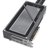
These pictures are for the convenience of volt modders and people who would like to see all the finer details on the PCB. Feel free to link back to us and use these in your articles, videos or forum posts.

High-resolution versions are also available (front, back).
Circuit Board (PCB) Analysis


GPU voltage is a massive 24-phase design managed by a Monolithic Power Systems MP2891 controller, which also handles memory voltage.

For the GPU voltage, Monolithic Power Systems MP86957 DrMOS chips are used; they are rated for up to 70 A output current each.

Memory voltage is a four-phase design, managed by the same MP2891 that's used for GPU voltage.

For memory, Monolithic Power Systems MP86957 DrMOS chips are used, again rated at 70 A.

The GDDR6X memory chips are made by Micron and carry the model number D8BZC, which decodes to MT61K512M32KPA-21:U. They are specified to run at 1313 MHz (21 Gbps effective).

NVIDIA's AD102 graphics processor is the company's flagship Ada Lovelace GPU. It's the world's first 5 nanometer GPU, built at TSMC Taiwan with a transistor count of 76.3 billion and a die size of 608 mm².
Jun 15th, 2024 18:05 EDT
change timezone
Latest GPU Drivers
New Forum Posts
- when using only 2 out of 4 ram slots which 2 are best? (3)
- Post your Speedometer 3.0 Score (46)
- Intel Optane 1TB (14)
- Amazing moderator acknowledgement (9)
- Can you help me decide for which AM4 CPU to buy plz? (18)
- new tv/display what one? what to avoid? (23)
- System shutdown from short when connecting USB type C cable? (20)
- LOL ASUS says this is $200 in repair, Steve from gamers Nexus smokes ASUS, Steam Deck til I die boys!!!! (151)
- A Final Fantasy IX Reminiscence - My love letter and homage to one of the best stories ever told (0)
- I should upgrade my gpu and psu? (10)
Popular Reviews
- Aune AR5000 Headphones + S17 Pro Headphones Amplifier Review
- Pulsar Xlite V3 eS Review
- VAXEE Outset AX Wireless (4K) Review
- Upcoming Hardware Launches 2024 (Updated May 2024)
- Team Group T-Force G70 Pro 2 TB Review
- Intel Lunar Lake Technical Deep Dive - So many Revolutions in One Chip
- AMD Ryzen 7 7800X3D Review - The Best Gaming CPU
- NZXT H6 Flow RGB Review
- Quick Look: Final UX2000 Wireless Noise Canceling Headphones
- Thermal Grizzly KryoSheet Review - Tested on RX 7900 XTX with 475 W
Controversial News Posts
- Possible Specs of NVIDIA GeForce "Blackwell" GPU Lineup Leaked (132)
- NVIDIA RTX 5090 "Blackwell" Founders Edition to Implement the "RTX 4090 Ti" Cinderblock Design (118)
- AMD Outs Ryzen 5000XT Processors for Socket AM4, an 8-year Old Socket (105)
- Nightmare Fuel for Intel: Arm CEO Predicts Arm will Take Over 50% Windows PC Market-share by 2029 (105)
- AMD Ryzen 9000 Zen 5 Single Thread Performance at 5.80 GHz Found 19% Over Zen 4 (103)
- AMD Says Ryzen 9000 Series Won't Beat 7000X3D Series at Gaming (101)
- AMD Zen 5 Storms into Gaming Desktops with Ryzen 9000 "Granite Ridge" Processors (100)
- Biden Administration to Revive Trump-Era Tariffs on China-made GPUs and Motherboards (95)