Report an Error
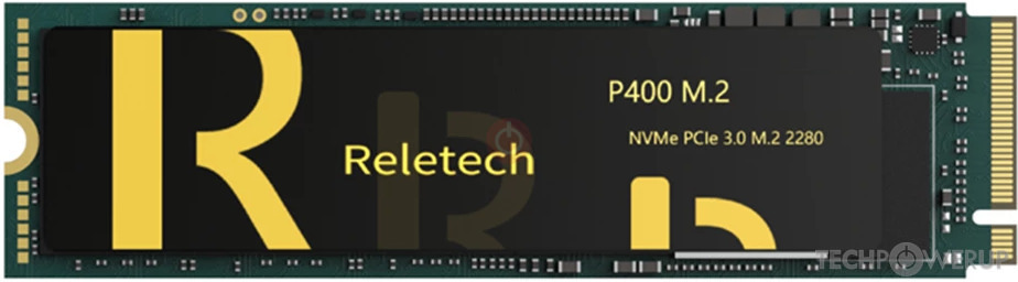
Reletech P400 256 GB (YMTC BCT1B)
256 GB
Capacity
Phison E12S
Controller
TLC
Flash
PCIe 3.0 x4
Interface
M.2 2280
Form Factor
Multiple hardware versions found.
Performance could vary due to unannounced flash/controller changes.
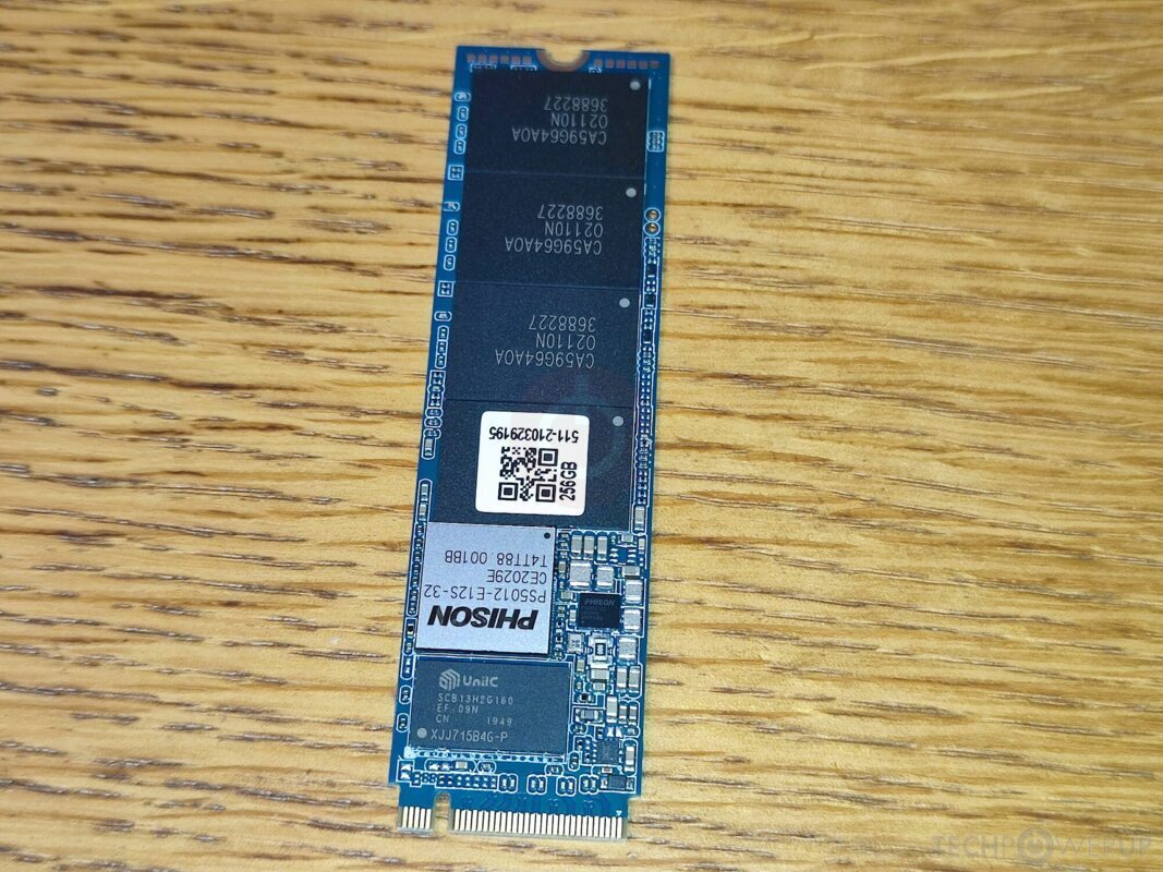
PCB Front

Controller

NAND Die
The Reletech P400 is a solid-state drive in the M.2 2280 form factor, launched in 2021. It is available in capacities ranging from 256 GB to 512 GB. This page reports specifications for the 256 GB variant. With the rest of the system, the Reletech P400 interfaces using a PCI-Express 3.0 x4 connection. The SSD controller is the PS5012-E12S-32 from Phison, a DRAM cache chip is available. Reletech has installed 64-layer TLC NAND flash on the P400, the flash chips are made by YMTC. Please note that this SSD is sold in multiple variants with different NAND flash or controller, which could affect performance, the "Notes" section at the end of this page has more info. To improve write speeds, a pseudo-SLC cache is used, so bursts of incoming writes are soaked up more quickly. The P400 is rated for sequential read speeds of up to 3,500 MB/s and 1,400 MB/s write.
At its launch, the SSD was priced at 41 USD. The warranty length is set to five years, which is an excellent warranty period. Reletech guarantees an endurance rating of 420 TBW, a good value.
At its launch, the SSD was priced at 41 USD. The warranty length is set to five years, which is an excellent warranty period. Reletech guarantees an endurance rating of 420 TBW, a good value.
Solid-State-Drive
| Capacity: | 256 GB |
|---|---|
| Variants: | 256 GB 512 GB |
| Hardware Versions: | |
| Overprovisioning: | 17.6 GB / 7.4 % |
| Production: | Active |
| Released: | 2021 |
| Price at Launch: | 41 USD |
| Part Number: | Unknown |
| Market: | Consumer |
Physical
| Form Factor: | M.2 2280 (Single-Sided) |
|---|---|
| Interface: | PCIe 3.0 x4 |
| Protocol: | NVMe 1.3 |
| Power Draw: | Unknown |
Controller
| Manufacturer: | Phison |
|---|---|
| Name: | PS5012-E12S-32 |
| Architecture: | ARM 32-bit Cortex-R5 |
| Core Count: | Quad-Core |
| Frequency: | 667 MHz |
| Foundry: | TSMC |
| Process: | 12 nm |
| Flash Channels: | 8 @ 667 MT/s |
| Chip Enables: | 4 |
| Controller Features: | DRAM (enabled) |
NAND Flash
| Manufacturer: | YMTC |
|---|---|
| Name: | Xtacking 1.0 |
| Part Number: | CA59G64AOA |
| Type: | TLC |
| Technology: | 64-layer |
| Speed: | 800 MT/s |
| Capacity: | 4 chips @ 512 Gbit |
| ONFI: | 4.0 |
| Topology: | Charge Trap |
| Process: | 40 nm |
| Die Size: | 58 mm² (4.4 Gbit/mm²) |
| Dies per Chip: | 2 dies @ 256 Gbit |
| Planes per Die: | 2 |
| Decks per Die: | 1 |
| Word Lines: |
73 per NAND String
87.7% Vertical Efficiency |
| Read Time (tR): | 74 µs |
| Program Time (tProg): | 760 µs |
| Block Erase Time (tBERS): | 9.0 ms |
| Die Read Speed: | 432 MB/s |
| Die Write Speed: | 42 MB/s |
| Endurance: (up to) |
1500 P/E Cycles |
| Page Size: | 16 KB |
| Block Size: | 1152 Pages |
| Plane Size: | 1006 Blocks |
DRAM Cache
| Type: | DDR3L-2133 CL18 |
|---|---|
| Name: | UniSemicon SCB13H2G160EF |
| Capacity: |
256 MB
(1x 256 MB) |
| Organization: | 2Gx16 |
Performance
| Sequential Read: | 3,500 MB/s |
|---|---|
| Sequential Write: | 1,400 MB/s |
| Random Read: | Unknown |
| Random Write: | Unknown |
| Endurance: | 420 TBW |
| Warranty: | 5 Years |
| MTBF: | 1.8 Million Hours |
| Drive Writes Per Day (DWPD): | 0.9 |
| SLC Write Cache: | Yes |
Features
| TRIM: | Yes |
|---|---|
| SMART: | Yes |
| Power Loss Protection: | No |
| Encryption: |
|
| RGB Lighting: | Unknown |
| PS5 Compatible: | No |
Notes
Controller:2 main cores using Cortex-R5 clocked at 667 MHz with CoXProcessor technology (one additional dual-core) Cortex-R5 clocked at a lower clock for better efficience. The difference between this revision and the E12 revision is that this has a nichel IHS to improve the temperature, a smaller size, smaller node (12nm TSMC FinFET) and this works with less DRAM capacity. NAND Die:Array Eficiency of over 90% |
Jun 14th, 2024 02:10 EDT
change timezone
Latest GPU Drivers
New Forum Posts
- Should i upgrade my cpu (rtx 4070) ? (5)
- Dell Workstation Owners Club (3109)
- GPU stuck in P0 state (10)
- PhysXs (3)
- Good Bronze 750w PSU (68)
- What do you mostly use your desktop PC for? (Pick your top 3!) (76)
- A good Linux Distro for AMD Athlon 64 X2 5200+ (7)
- What phone you use as your daily driver? And, a discussion of them. (1542)
- 9900X3D - Will AMD solve the split CCD issue (261)
- TPU's Nostalgic Hardware Club (18580)
Popular Reviews
- VAXEE Outset AX Wireless (4K) Review
- Pulsar Xlite V3 eS Review
- Aune AR5000 Headphones + S17 Pro Headphones Amplifier Review
- Upcoming Hardware Launches 2024 (Updated May 2024)
- Intel Lunar Lake Technical Deep Dive - So many Revolutions in One Chip
- AMD Ryzen 7 7800X3D Review - The Best Gaming CPU
- Quick Look: Final UX2000 Wireless Noise Canceling Headphones
- NZXT H6 Flow RGB Review
- Pulsar Xlite V3 Review
- Thermal Grizzly KryoSheet Review - Tested on RX 7900 XTX with 475 W
Controversial News Posts
- Possible Specs of NVIDIA GeForce "Blackwell" GPU Lineup Leaked (131)
- NVIDIA RTX 5090 "Blackwell" Founders Edition to Implement the "RTX 4090 Ti" Cinderblock Design (118)
- Nightmare Fuel for Intel: Arm CEO Predicts Arm will Take Over 50% Windows PC Market-share by 2029 (105)
- AMD Zen 5 Storms into Gaming Desktops with Ryzen 9000 "Granite Ridge" Processors (100)
- Biden Administration to Revive Trump-Era Tariffs on China-made GPUs and Motherboards (95)
- ASRock Innovates First AMD Radeon RX 7000 Graphics Card with 12V-2x6 Power Connector (94)
- AMD Ryzen 9000 Zen 5 Single Thread Performance at 5.80 GHz Found 19% Over Zen 4 (92)
- AMD Outs Ryzen 5000XT Processors for Socket AM4, an 8-year Old Socket (84)