Wednesday, July 29th 2009

Clarkdale 3.06 GHz Faces a Preview, Series Pricing Surfaces
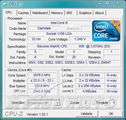
"Clarkdale" is the codename for Intel's upcoming dual-core processors derived from the Nehalem/Westmere architecture. The move marks a leap for Intel in two ways: introducting the first commercial-grade 32 nm microprocessor, and implementing a radical new design that involved relocating the platform's northbridge component entirely to the CPU package. Slated for Q1 2010, Clarkdale will go by three brand indentifiers to grade it according to a performance and feature scale. You have the Core i5 class that enables the entire feature-set of processor, there's the Core i3 class that offers some features, excluding Intel Turbo Boost technology for example, finally there's the sub-$100 Pentium part (yes, Pentium lives on), which offers a smaller feature-set. HyperThreading technology is disabled on this one.
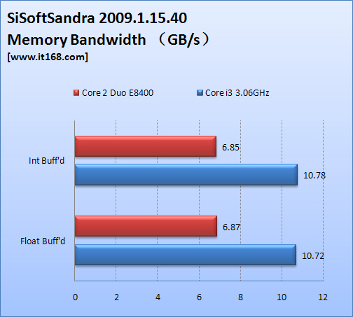
Chinese tech-site IT168 published a comprehensive performance (p)review of the 3.06 GHz Clarkdale part. In the article, the 3.06 GHz Clarkdale was pitted against the 3.00 GHz "Wolfdale" Core 2 Duo processor. The memory (Dual-channel DDR3-1333, 4 GB) and graphics hardware (ATI Radeon HD 4870, 1 GB) were kept common between the two test-beds. Tests ranged from memory and CPU internal bandwidth tests, math-intensive tests, synthetic multimedia and 3D tests, and finally, modern 3D games.
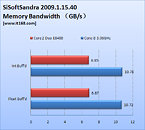
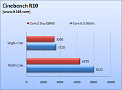 With an integrated memory controller, Clarkdale is swimming in higher bandwidth, and lower latency compared to its predecessor, as tested on SANDRA 2009. Having four threads on two cores thanks to HyperThreading, however, doesn't seem to have a significant impact on its performance at the multi-threaded Cinebench R10. Even at the single-core run, the increment is passable at best.
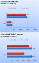
Notable CPU benchmarks from Everest 5, the CPU Z-lib and FPU Julia series (Julia and Sin-Julia) is where the new chip seems to shine with significant increments. A roughly 40 percent increment at Z-lib, and a healthy 90+ percent boost with Sin Junlia. Clarkdale churns out surprisingly high scores with 3DMark Vantage (CPU test), something it doesn't manage with 3DMark06.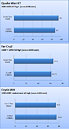
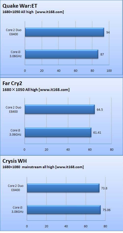
If purely gaming is your thing, and you have a current generation machine, these charts will interest you. Popular games such as Enemy Territory: Quake Wars, Far Cry 2, and Crysis Warhead show the two chips to be performing neck and neck.
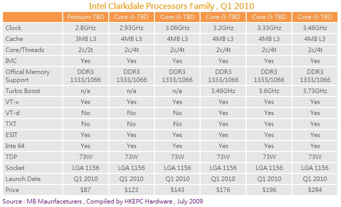
In related news, HKEPC compiled a neat table listing out Intel's first-wave of Clarkdale-based processors, starting from the sub-$100 Pentium, to the entry-mainstream Core i3, and over to the mainstream-performance Core i5. The models and their tentative prices were sourced from motherboard manufacturers. A bulk of the lineup is positioned in the $126~$196 range. At these prices, they share space with at least one quad-core LGA-1156 processor, the 2.66 GHz Core i5 "Lynnfield" 750, while the 3.46 GHz Clarkdale will be locking horns with the 2.80 GHz Lynnfield at the ~$280 price point. IT168's complete review Google-translated to English can be read here.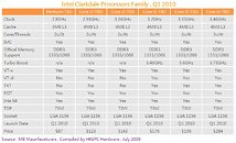
Sources:
IT168, HKEPC
Chinese tech-site IT168 published a comprehensive performance (p)review of the 3.06 GHz Clarkdale part. In the article, the 3.06 GHz Clarkdale was pitted against the 3.00 GHz "Wolfdale" Core 2 Duo processor. The memory (Dual-channel DDR3-1333, 4 GB) and graphics hardware (ATI Radeon HD 4870, 1 GB) were kept common between the two test-beds. Tests ranged from memory and CPU internal bandwidth tests, math-intensive tests, synthetic multimedia and 3D tests, and finally, modern 3D games.


In related news, HKEPC compiled a neat table listing out Intel's first-wave of Clarkdale-based processors, starting from the sub-$100 Pentium, to the entry-mainstream Core i3, and over to the mainstream-performance Core i5. The models and their tentative prices were sourced from motherboard manufacturers. A bulk of the lineup is positioned in the $126~$196 range. At these prices, they share space with at least one quad-core LGA-1156 processor, the 2.66 GHz Core i5 "Lynnfield" 750, while the 3.46 GHz Clarkdale will be locking horns with the 2.80 GHz Lynnfield at the ~$280 price point. IT168's complete review Google-translated to English can be read here.
31 Comments on Clarkdale 3.06 GHz Faces a Preview, Series Pricing Surfaces
Don't get me wrong these look great, but untill they face a real world set of tests from a few sites this is all fluff.
why no quad core westmere so far? en.wikipedia.org/wiki/Intel_Nehalem_%28microarchitecture%29#32_nm_.22Westmere.22 they made dualcore clarkdale and hexacore gulftown but no quads so far:(
I can only hope AMD will come up with something and influence the prices or even put out some affordable 32 nm quads... we'll see I guess.
Maybe we'll see better results with the nextgen of video cards and mature non-ES cpus ?
But I will still buy the cheapest one and see if I could get 5.0Ghz out of it.
"The memory controller, which handles communication between the CPU and RAM, has been moved onto the processor die in AMD64 processors. Intel has integrated the memory controller onto the processor die with their Nehalem microarchitecture-based processors.
Another example of this kind of change is NVIDIA's nForce3 chipset for AMD64 systems that is a single chip. It combines all of the features of a normal southbridge with an AGP port and connects directly to the CPU. On nForce4 boards they consider this to be an MCP (Media Communications Processor)."
I am not trying to argue, just learn and understand. In that case, the GPU and Memory controllers would both be on the CPU for the i3. Is that right?
All AMD did was split the northbridge to two, take the memory controller component onto the CPU, while the rest of it stayed on as the motherboard chipset, with HyperTransport connection between the two "halves". Now that half can remain as a lesser motherboard northbridge (as with present AMD 7-series chipsets) or unify with the southbridge in a single chip design (as with present nForce 700a series chipsets).
Intel completely relocated the northbridge to the CPU package, so now the package needs only a 2 GB/s DMI connection with all that remains on the board as "chipset", which is the Intel 5-series chipset, Intel P/H/G-55/57 is what Intel calls a PCH "peripheral hub?", which is just a glorified southbridge.
Hope this helps you understand: img.techpowerup.org/090729/btacpuarch1.png
The original definition of northbridge, was the chip with the memory controller - hence the confusion when discussing it.
Good move on Intel to scrap the 45nm Havendale, they would have been even less of an upgrade and more expensive to make.