Thursday, June 17th 2010

Toshiba Launches Industry's Largest Embedded NAND Flash Memory Modules
Toshiba America Electronic Components, Inc.(TAEC) and its parent company Toshiba Corporation today announced the launch of a 128-gigabyte (GB) embedded NAND flash memory module, the highest capacity yet achieved in the industry. The module is fully compliant with the latest e-MMC standard, and is designed for application in a wide range of digital consumer products, including smartphones, tablet PCs and digital video cameras. Samples will be available in September, and mass production will start in the fourth quarter (October to December) of 2010.
The new 128GB embedded device integrates sixteen 64Gbit (equal to 8GB) NAND chips fabricated with Toshiba's cutting-edge 32nm process technology and a dedicated controller into a small package 17 x 22 x 1.4mm. Toshiba is the first company to succeed in combining sixteen 64Gbit NAND chips, and applied advanced chip thinning and layering technologies to realize individual chips that are only 30 micrometers thick.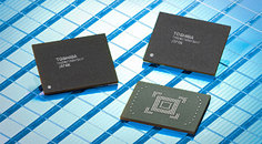 Toshiba offers a comprehensive line-up of single-package embedded NAND Flash memories in densities from 2GB to 128GB. They integrate a controller to manage basic control functions for NAND applications, and are compatible with the JEDEC e-MMC Version 4.4 and its new features. New samples of 64GB chips will also be available from August.
Demand continues to grow for large density chips that support high-resolution video and deliver enhanced storage, particularly in the area of embedded memories with a controller function that minimize development requirements and ease integration into system designs. Toshiba has established itself as an innovator in this key area, and is now reinforcing its leadership by being first to announce a 128GB generation module.
Key Features
The new 128GB embedded device integrates sixteen 64Gbit (equal to 8GB) NAND chips fabricated with Toshiba's cutting-edge 32nm process technology and a dedicated controller into a small package 17 x 22 x 1.4mm. Toshiba is the first company to succeed in combining sixteen 64Gbit NAND chips, and applied advanced chip thinning and layering technologies to realize individual chips that are only 30 micrometers thick.

Demand continues to grow for large density chips that support high-resolution video and deliver enhanced storage, particularly in the area of embedded memories with a controller function that minimize development requirements and ease integration into system designs. Toshiba has established itself as an innovator in this key area, and is now reinforcing its leadership by being first to announce a 128GB generation module.
Key Features
- The JEDEC e-MMC V4.4 compliant interface handles essential functions, including writing block management, error correction and driver software. It simplifies system development, allowing manufacturers to minimize development costs and speed time to market for new and upgraded products.
- The 128GB device stacks sixteen 64Gbit chips fabricated with leading-edge 32nm process technology. Application of advanced chip thinning, layering and wire bonding technologies has allowed Toshiba to achieve individual chips only 30 micrometers thick, and to layer and bond them in a small package. The result is an embedded flash memory module with the industry's highest density.
- The new products are sealed in a small FBGA package only 17 x 22 x 1.4mm and has a signal layout compliant with the JEDEC e-MMC V4.4.

3 Comments on Toshiba Launches Industry's Largest Embedded NAND Flash Memory Modules
AND SMASH IT AGAINST THE FIRST IPAD I SEE!!!! :rockout: