Monday, September 27th 2010

AMD Radeon HD 6700 Series ''Barts'' Specs Sheet Surfaces

Here is the slide we've been waiting for, the specs sheet of AMD's next-generation Radeon HD 6700 series GPUs, based on a new, radically redesigned core, codenamed "Barts". The XT variant denotes Radeon HD 6770, and Pro denotes HD 6750. AMD claims that the HD 6700 series will pack "Twice the Horsepower", over previous generation HD 5700 series. Compared to the "Juniper" die that went into making the Radeon HD 5700 series, Barts features twice the memory bandwidth thanks to its 256-bit wide high-speed memory interface, key components such as the SIMD arrays split into two blocks (like on Cypress), and we're now getting to learn that it uses a more efficient 4-D stream processor design. There are 1280 stream processors available to the HD 6770 (Barts XT), and 1120 stream processors to the HD 6750 (Barts Pro). Both SKUs use the full 256-bit memory bus width.

The most interesting specification here is the shader compute power. Barts XT churns out 2.3 TFLOP/s with 1280 stream processors, GPU clocked at 900 MHz, while the Radeon HD 5870 manages 2.72 TFLOP/s with 1600 stream processors, 850 MHz. So indeed the redesigned SIMD core is working its magic. Z/Stencil performance also shot up more than 100% over the Radeon HD 5700 series. Both the HD 6770 and HD 6750 will be equipped with 5 GT/s memory chips, at least on the reference-design cards, which are technically capable of running at 1250 MHz (5 GHz effective), though are clocked at 1050 MHz (4.20 GHz effective) on HD 6770, and 1000 MHz (4 GHz effective) on HD 6750. Although these design changes will inevitably result in a larger die compared to Juniper, it could still be smaller than Cypress, and hence, more energy-efficient.
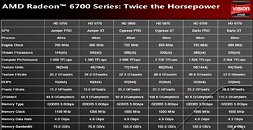
Source: PCinLife
Add your own comment

245 Comments on AMD Radeon HD 6700 Series ''Barts'' Specs Sheet Surfaces

#76
Yellow&Nerdy?
I see what AMD is doing here. Because the thermal performance on the current Nvidia top-cards is so bad, they can loosen up their standards too and concentrate on performance instead. So what the 68** series cards will probably be is a slightly smaller and slightly more power-efficient than GF100, but with better performance. As for the 6970 goes, nobody knows...

But personally, I don't think that AMD will be able to pull off the 5850 -> 6770, 5970 - > 6870 and so on. Although all the uncore parts on the chips are new, it's still 40nm. I would expect the 6850 to be between the 5870 and the GTX 480/very close to the GTX 480 and the 6870 to be somewhere between the GTX 480 and the 5970. I just hope they don't go coocoo bananas on the price...
Posted on Reply
#77
douglatins
I want a properly cooled dual card, like the rev2 of the GTX 295 or like the XFX 5970 gun one
Posted on Reply
#78
SNiiPE_DoGG
In this chart posted the Tflops columns of the 5850/5870 are switched with the Tflops of the 6750/6770... no?

they are the only specs for each card that are out of line....
Posted on Reply
#79
laszlo
i expect disappointing performance considering is equal to cypress almost on paper just my opinion
Posted on Reply
#80
erocker
*
laszloi expect disappointing performance considering is equal to cypress almost on paper just my opinion
These new cards on the chart are the mid-range models, replacing the 5750 and 5770 models. The 5850 and 5870 replacement specs are not known yet.

* @ Paintface If 6770 is $199 and 6750 is $159 it will be win. However, ATi erm.. AMD has been a little greedy in their pricing so who knows.
Posted on Reply
#81
Paintface
now big question is price , will we see barts XT performance wise between 5850 and 5870 for less than 200 at launch?
Posted on Reply
#82
dj-electric
wow those specs are really really amazing, i did not expected over 33% increase in performance on this gpu gen
Posted on Reply
#83
Completely Bonkers
I would have rather have seen a 70% improvement in performance and a 30% reduction in power, to a sub 80W card, running nearly silently. Not only would it be more suitable for my purposes, it would have been a great signal to the industry... low power is good.

Nonetheless, 6770 looks good.
Posted on Reply
#84
cheezburger
BenetanegiaIf you want to avoid my post, bottom line is Nvidia is not in trouble at all, in fact it is in a much better position than it was with GF100.

Nvidia and AMD have several teams working on different chips and generations of chips, so the fact that one chip is late doesn't affect others. It does shake the next releases a bit but mostly from a marketing standpoint, as they first want to sell some high-end chips, before they release the perf/price king (i.e GF100->GF104 == G80->G92). The original schedule in Nvidia was GF100 in Q4 2009, GF104 in Q1 2010 and mainstream/entry in Q2, rinse and repeat with next gen starting in Q4 2010. So basically GF100 was late by 6+ months, GF104 was late by 3 months and GF106 by 2 months or so. Next gen is not going to be late necessarily or too late, i.e Q1 2011 release. Remember that Nvidia doesn't need any re-design at the moment, they just need to add clusters or SIMDs to GF104 and have a "winner" in comparison to GF100 and that should be enough to compete with HD6000 cards.

For example, without engineers et all thinking too much (nothing at all actually :laugh:), adding one more cluster to GF104 you end up with a chip slightly smaller than GF100 (less than 3 billion transistors against the 3+ billion in GF100) but with significantly better specs:

Shaders: 480 SP -> 576 SP, 20% increase*
texture units: 64 TMU -> 96 TMU, 50% increase*
ROP: 48 same*
memory: 384 bit same*

* That's without taking into account that GF104 clocks much better than GF100, the new chip could be clocked at 800 Mhz easily and that would mean the new chip would be 30-40% faster than the GTX480, soundly beating the HD5970 and probably the HD6870 by the same ammount as the GTX480 beats the HD5870, except this time Cayman is said to be 400mm and NV chip would be a bit smaller than GF100.

On top of that and considering that finally TSMC's 40nm is at same yields as 55nm, Nvidia could decide to take the risk and instead of releasing a slightly smaller chip, they could go with a slightly bigger, but yummy yummy, chip. How? Same chip as mentioned above except they'd add one more SIMD to the SMs (note how small a cange this is and how easy to engineer/release it would be). GF104 is superscalar and its SMs have 3 SIMDS while having 2 schedulers, wasting one scheduler every odd clock cycle because it has no SIMD unit to talk to. The jump to 4 SIMDs at some point is unavoidable then, why not do it now, taking a small risk**? End result (and compared to GTX480):

764 SPs (+60%), 96 TMU (+50%), 48 ROPs, 384 bit. 750 Mhz...

** Small, because at this point 40nm yields are good, they know the process better and the resulted chip I estimate it would have 3.2 billion transistors and be smaller than GT200 in 65nm. That is, it wouldn't be the biggest chip Nvidia has made, but the benefits are enormous.
768 cuda: 96TMU:48rops 384bit bus and 750mhz core clock.....

i wouldn't imagine the die size of this monster....perhaps 600mm^2? serious either cayman and fermi 2's shader had gone way too ridiculous in number....if cayman is 640 ALU with 484mm^2 die space i can't imagine fermi 2 will be any size below 600mm^2...
Paintfacenow big question is price , will we see barts XT performance wise between 5850 and 5870 for less than 200 at launch?
no barts pro is out pace 5870 already and barts xt may be competitive with gtx 470/480. according the benchmark from chiphell.
Posted on Reply
#85
dalelaroy
Barts Positioning
calebIs the 6750 a next 5750 or 5850 ?
This naming scheme is starting to be confusing
The Radeon HD 6750 is the new Radeon HD 5830. It is to be positioned against the GTX 460 768.

The Radeon HD 6670 (Turks) will be the new Radeon HD 5750. It will offer the DX 9/10 performance of the Radeon HD 4770 and DX 11 performance midway between that of the Radeon HD 5750 and Radeon HD 5770 at the $99 price of the Radeon HD 4770.

In short Turks will edge out the performance of the GTS 450 using less than the 75 watts of the PCIe slot while costing less than $100.
Posted on Reply
#86
LAN_deRf_HA
Don't want to start an argument, just pointing out that if you haven't encountered much in the way of ati driver issues try dealing in larger volumes. I used to always use nvidia cards in my builds because people preferred the brand and the experience was just slightly smoother on the low-mid end at the time. Then everyone, and I mean like 99% of clients, started hooking these things up to HDTVs. It looks like shit and they sit 2 ft away but w/e. So I switched to ati because the HDTV experience was much nicer with them. Plug and play and you even got sound out by default. I also got a noticeable increase in bugs. Bear in mind these were always fresh installs. If it wasn't flash incompatibilities crashing the whole system it was graphical errors in games. Luckily I've found they'd fix these issues with time. It just often took 4 driver releases to address some of these things. Yeah nvidia apparently has bugs, but I never ran into them. So comparing the two, I'd say they probably have the same amount of driver issues, it's just that nvidia's seem to be more obscure.
Posted on Reply
#87
3volvedcombat
All these people fighting for ATI's Drivers and trying to be legitimate on that there good drivers.

I know, there problems that are rediculas because of ATI drivers, When using a great dx11 5850 or 5870, and yet people have to take there time out of there life, to go try to find fixes to some games, and probably future games.

It doesn't matter if its just 1 game, or 20 games having issue's and needing refreshed hot-fixes because all cards arnt supported.

With all the flow of cash, and rep, they need to completely re-change there driver scheme.

I know, I really enjoy, just grabbing a nvidia card, updated the driver base from nvidia, and just plugging it in, having it already recognized, and ready to push fps in games.

Never having to ever go in the control panel, to edit some AA settings, shut off some extra video processing settings for some old games, or having rediculas forcing issue's.

nvidia's drivers are really solid, And on the ati side, Ive seen the problems, so many of them, People strive to go download like 10 diffrent 10.xx- to 10.8x drivers to see which one is the most stable and best performing.

I really never see that with nvidia drivers, cause there all basic, there all solid performing, realiable, easy to use, and dependably stable drivers 85-95% of the time.

on ati's case, that isn't so much the same.

My friend decided to crap shoot his perfect 1gb 4870's and begged me for my old gtx 260.

Many people come in my computer shop, say they have had to tweak some in the ccc, or forced to, after googling the problem, to play the game.
Posted on Reply
#88
alwayssts
20mmrainSo from what I can tell the 6770 will be around a 5850/5870 performance area? And the 6750 will be around the 5830/5850 performance area?

With powerful enough tessellation (Rumored) to take down the GTX 400 series. Man if this is the case... why spend $599 for a 6870 when you could get two of these trounce a 6870 and be able to play any game out there.

Hope fully they won't make it like Nvidia did and only have it two way Xfire/SLI. Because if they allowed 3-way.... while it might hurt 6870 sales.... it would kill any GTX 460 sales for sure! I thought that was the whole Idea of releasing these cards first anyway's wasn't it?
The engineering sample pics show that's exactly what they're doing. This range is limited to 2-way crossfire. Like you infer, 2-way will likely beat one 6800-series product for a similar amount of money, give or take the benefits of a single card versus crossfire scaling and minimum frame rates. The question is does AMD take that hit against the 6800 series or do they price the 6700 series higher to avoid it? If they do price it higher, they risk allowing GF104 parts room to breathe and take those sales for the budget-conscious bang-for-buckers. I personally think they'll look at as it's okay for the 6700 series crossfire to compare/beat Cayman on bang-for-buck, but avoiud cannibalizing 6800-series crossfire configurations or the COAS (X2) part. Hence, only 2-way. Barts may start with a higher price-tag, but I'll bet supply/demand forces them down to the ~$150/200 price range to annihilate the GTX460.

I wonder when it'll be safe to assume Turks is 640sp/16R/32TMU/128-bit? Smart on AMD's part if they are going this route. Evergreen was 1/4-1/2-1/1 parts in a series while NI looks to be 1/3, 2/3, 1/1 (granted likely without the added ROPs and mem controller on Cayman).

Hope that each 640sp (8 SIMDs) cluster has it's own setup engine to go along with such a possible divide. If they split tessellation up like that, Barts would be similar to GF104; Turks similar to GF106 with 2 and 1 triangles per clock respectively. Cayman would be interesting. While GF100 does supposedly 4 triangles per clock, if 6870 did 3 and was clocked at 900mhz, GTX480/6870 would essentially be equal in theoretical triangle output. [Math = (.75X900)/700 = 96%]. Obviously implementation and technique come into play, but it's interesting that AMD may use less transistors and the clock/watt allowances of 40nm to perhaps achieve the same stock result with less power consumption.
Posted on Reply
#89
Benetanegia
cheezburger768 cuda: 96TMU:48rops 384bit bus and 750mhz core clock.....

i wouldn't imagine the die size of this monster....perhaps 600mm^2? serious either cayman and fermi 2's shader had gone way too ridiculous in number....if cayman is 640 ALU with 484mm^2 die space i can't imagine fermi 2 will be any size below 600mm^2...
IMO no, not at all. I was thinking about something like 560 mm^2 max (but I'm even questioning that after writing this post, it could actually be smaller!!). It's not GF100 based, but an evolution based on GF104. Remember how I came up with those numbers.

1- First of all the only thing that I did was to add one more cluster to GF104. That already means 576 SP: 96TMU: 48 ROPS: 384 bit. That is exactly 1.5x GF104 or 2.925 billion transistors. Compared to the 3+ billions on GF100, thats actually a 5% reduction. Let's call this one Prototype A.

2- GF104 has same ammount of TMUs and SFUs as GF100 and 75% of the cuda cores, it also has 66% of the ROPs and memory bus. The end result is a chip that has 66% as many transistors, meaning that the extra cuda cores, TMUs and SFUs don't affect transistor count or die area too much, if at all, as long as they are included in existing SMs. To come up with the 768 SP number the only thing you have to do is add another 16 way SIMD unit to each Shader Multiprocessor in Prototype A, which is exactly one of the things of what was done between GF100 and GF104. That's why I said it would be slightly bigger than GF100, but TBH after figuring out both 66% numbers above, how they seem to be related, and how adding all those extra TMUs and SFUs and cuda cores didn't impact die area at all, I even have to question my first judgement on that. The more I think about it, the more I think that Nvidia might be able to create that 768 SP monster in the same die area or less!! than GF100.
Posted on Reply
#90
cheezburger
BenetanegiaIMO no, not at all. I was thinking about something like 560 mm^2 max (but I'm even questioning that after writing this post, it could actually be smaller!!). It's not GF100 based, but an evolution based on GF104. Remember how I came up with those numbers.

1- First of all the only thing that I did was to add one more cluster to GF104. That already means 576 SP: 96TMU: 48 ROPS: 384 bit. That is exactly 1.5x GF104 or 2.925 billion transistors. Compared to the 3+ billions on GF100, thats actually a 5% reduction. Let's call this one Prototype A.

2- GF104 has same ammount of TMUs and SFUs as GF100 and 75% of the cuda cores, it also has 66% of the ROPs and memory bus. The end result is a chip that has 66% as many transistors, meaning that the extra cuda cores, TMUs and SFUs don't affect transistor count or die area too much, if at all, as long as they are included in existing SMs. To come up with the 768 SP number the only thing you have to do is add another 16 way SIMD unit to each Shader Multiprocessor in Prototype A, which is exactly one of the things of what was done between GF100 and GF104. That's why I said it would be slightly bigger than GF100, but TBH after figuring out both 66% numbers above, how they seem to be related, and how adding all those extra TMUs and SFUs and cuda cores didn't impact die area at all, I even have to question my first judgement on that. The more I think about it, the more I think that Nvidia might be able to create that 768 SP monster in the same die area or less!! than GF100.
we all know cuda take about 65~70% of die space in both g100 and g104. which g104 is 336 cuda with about 367mm^2 die space and 336 cuda ALU took 367mm^2 x 0.65 = 238.55mm^2..consider 768 is about 2.28x of space along...without counting the transistor that form SIMD cluster/rops/ram bus and texture mapping unit. the tmu/SIMD controller from g100/104 is about 10% of die space which make a g104's tmu about 367mm^2 x 5% = 36.70mm^2. if we increase the tmu from 60 to 96..about 60% increase 36.7mm^2 x 1.6 = 58.72mm^2..while if rops/bus won't change the die size will be come like below:

rop/bus = 20% of g100 = 529mm^2 x 0.2 = 105.8mm^2

SIMD/TMU increase from 60 to 96 = 36.70mm^2 x 1.6 = 58.72mm^2

CUDA increase from 336 to 768 = 338.55mm^2 x 2.28 = 545.257mm^2

(105.8mm^2 + 58.72mm^2 + 545.257mm^2) X105%(hard wiring )= 745.26mm^2.....

that is huge.....pretty much the largest GPU ever exist...not slightly but completely buffer up..

PS: under 28nm it will be another store....may be it can only happen on 28nm??

745.26mm^2 x (28nm/40nm)^2= 365.17mm^2

however amd can do exactly same with everything double up again...

cayamn in 28nm = 484mm^2 x (28nm/40nm)^2 = 237.16...so end up a hd 7878 with 128rops will be 484mm^2 again in 28nm...
Posted on Reply
#91
bear jesus
I have to admit all these "leaked" spec are making me hope that the referance coolers (at least for the high end models) are all vapour chamber baised coolers as i would assume that would help out with the cooling of what i would expect to be some hotter cards than the 5xxx.
Posted on Reply
#92
cadaveca
My name is Dave
Prertty sure all high-end AMD gpus will feature Vapor-Chamber coolers...didn't AMD help develop that tech, or buy it or something?

Cards sound exciting, it's just really hard for me to get excited about them at all.
Posted on Reply
#93
Benetanegia
cheezburgerwe all know cuda take about 65~70% of die space in both g100 and g104. which g104 is 336 cuda with about 367mm^2 die space and 336 cuda ALU took 367mm^2 x 0.65 = 238.55mm^2..consider 768 is about 2.28x of space along...without counting the transistor that form SIMD cluster/rops/ram bus and texture mapping unit. the tmu/SIMD controller from g100/104 is about 10% of die space which make a g104's tmu about 367mm^2 x 5% = 36.70mm^2. if we increase the tmu from 60 to 96..about 60% increase 36.7mm^2 x 1.6 = 58.72mm^2..while if rops/bus won't change the die size will be come like below:

rop/bus = 20% of g100 = 529mm^2 x 0.2 = 105.8mm^2

SIMD/TMU increase from 60 to 96 = 36.70mm^2 x 1.6 = 58.72mm^2

CUDA increase from 336 to 768 = 338.55mm^2 x 2.28 = 545.257mm^2

(105.8mm^2 + 58.72mm^2 + 545.257mm^2) X105%(hard wiring )= 745.26mm^2.....

that is huge.....pretty much the largest GPU ever exist...not slightly but completely buffer up..

PS: under 28nm it will be another store....may be it can only happen on 28nm??

745.26mm^2 x (28nm/40nm)^2= 365.17mm^2

however amd can do exactly same with everything double up again...

cayamn in 28nm = 484mm^2 x (28nm/40nm)^2 = 237.16...so end up a hd 7878 with 128rops will be 484mm^2 again in 28nm...
Sorry I stopped paying attention after the first line, because it would be pointless. GF104 has 384 CUDA cores, with one SM, 48 SPs being disabled.

Have you read my post at all? Why are you adding A LOT of die area based on linear SP/TMU/etc. increase?? Like I said in GF104 Nvidia added many SPs and TMUs over the hypothetical 66% of a GF100 chip and that did not add any transistor.

I did my numbers too and the resulted die area is 520mm^2. Of course it's almost as arbitrary as yours, but at least is based on the correct number os SP/TMU in GF104 and I'm not basing it on how much area each unit takes ion GF100, because it's not going to be based in GF100... :shadedshu

And just to see how stupid your numbers are, let's calculate Bart and Cayman shall we?

Barts: It's almost a Cypress, except the shaders are 4D instead of 5D. So the shader/tmu area is 80% that of Cypress, everything else being equal.

Cypress was 2xRV770

img.chw.net/sitio/breves/200812/23_RV770_900SP.jpg

and as you can see the SP area is like 1/3 the chip. So (336*2/3) + (0.8*336/3) = 313mm^2

Cayman is twice that (or so they say) so: 626mm^2 man that is HUGE!
Posted on Reply
#94
bear jesus
cadavecaPrertty sure all high-end AMD gpus will feature Vapor-Chamber coolers...didn't AMD help develop that tech, or buy it or something?

Cards sound exciting, it's just really hard for me to get excited about them at all.
I don't know who developed them but witht he 5xxx card's i thought it was said they woudl be using a new cooling tech but then only the 5970 had a vapour chamber but if i remember correctly leaked pictures of a low end 6xxx card's passie cooler had one.

I have to admit i am excited but not just for the 6xxx cards, im excited upbout my next upgrades so that includes the 6xxx and 7xxx cards from amd, the 580 and 680 (assuming) from nvidia, intel's sandy bridge and amd's bulldozer, there is so much next gen hardware coming out over the next year or 2 that will be perfect to replace my current setup and move onto something insanly powerful even if i don't need that much power and then maybe do it again in about a year or so just for fun :D
Posted on Reply
#95
Drac
I cant imagine how will be the perfomance with less than 40 nm, this is just awesome.
My future mental list is motherboards with 16 cores CPU and 32 gb GDDR5(cya ddr3) and a 7XXX xd
Posted on Reply
#96
cadaveca
My name is Dave
bear jesusI have to admit i am excited but not just for the 6xxx cards, im excited upbout my next upgrades so that includes the 6xxx and 7xxx cards from amd, the 580 and 680 (assuming) from nvidia, intel's sandy bridge and amd's bulldozer, there is so much next gen hardware coming out over the next year or 2 that will be perfect to replace my current setup and move onto something insanly powerful even if i don't need that much power and then maybe do it again in about a year or so just for fun :D
It is just really shocking to me for them to exceed Moore's Law by reducing the time to double computational power by half.

It's almost too fast...software has issues keeping up as it is...

As it is now, I hopped on the Eyefinity bandwagon on launch of the 5-series, so I really cannot make any purchases until I see how Eyefinity performs, and if some of the bugs that are left still existing now are gone...this damn corrupting cursor is a real pain in the ass.
Posted on Reply
#97
jaredpace
Barts = HD 6800 series

NDA is Oct. 21


Posted on Reply
#99
EastCoasthandle
I would like for him to point out and quote specifically the portion of both pics that shows a bart as a 6800 series...
Posted on Reply
#100
cheezburger
BenetanegiaSorry I stopped paying attention after the first line, because it would be pointless. GF104 has 384 CUDA cores, with one SM, 48 SPs being disabled.

Have you read my post at all? Why are you adding A LOT of die area based on linear SP/TMU/etc. increase?? Like I said in GF104 Nvidia added many SPs and TMUs over the hypothetical 66% of a GF100 chip and that did not add any transistor.

I did my numbers too and the resulted die area is 520mm^2. Of course it's almost as arbitrary as yours, but at least is based on the correct number os SP/TMU in GF104 and I'm not basing it on how much area each unit takes ion GF100, because it's not going to be based in GF100... :shadedshu

And just to see how stupid your numbers are, let's calculate Bart and Cayman shall we?

Barts: It's almost a Cypress, except the shaders are 4D instead of 5D. So the shader/tmu area is 80% that of Cypress, everything else being equal.

Cypress was 2xRV770

img.chw.net/sitio/breves/200812/23_RV770_900SP.jpg

and as you can see the SP area is like 1/3 the chip. So (336*2/3) + (0.8*336/3) = 313mm^2

Cayman is twice that (or so they say) so: 626mm^2 man that is HUGE!
sry may be a little bit incorrect. ok let's do it again. 384cuda took 70% of die on g104 and 10% on SIMD/TUMU and @)% on rops/bus. then we put these to together and speculate how big fermi 2 will be:

2(367x0.7) + (367x0.1)x1.5 + (367x0.2)x1.5 = 678.95mm^2 x 10⁵%(hard wiring) = 713mm^2

cayman has 60% die space that fill with shader/ALU and 25% for rops/bus and 15% for TMU/SIMD

2(336x 0.6 x0.8) + 2(336 x 0.1) + 2(336x0.25) = 2x 278.88= 557.76mm^2 x 110% hard wiring(512bit bus)= 613mm^2

result...these two are ridiculously big..........

but if cayman is 1920:96:64 +512bit bus instead of double up it will be

1.5(336x0.6x0.8) +1.5(336x0.1) + 2(336x0.25)= 376.32mm^2 x 110% hard wiring for ram/bus optimization (512bit bus)= 413mm^2 for cayman

lets go back to fermi 2 if it's cuda number are 576 instead of crazy 768

1.2(367x0.7) + 1.5(367 x 0.1) + 1.5(336x0.15)= 473.43

which ALU are the reason why gpu can be oversize...
Posted on Reply
Add your own comment
Apr 25th, 2024 11:40 EDT change timezone

New Forum Posts

Popular Reviews

Controversial News Posts