Monday, September 27th 2010

AMD Radeon HD 6700 Series ''Barts'' Specs Sheet Surfaces

Here is the slide we've been waiting for, the specs sheet of AMD's next-generation Radeon HD 6700 series GPUs, based on a new, radically redesigned core, codenamed "Barts". The XT variant denotes Radeon HD 6770, and Pro denotes HD 6750. AMD claims that the HD 6700 series will pack "Twice the Horsepower", over previous generation HD 5700 series. Compared to the "Juniper" die that went into making the Radeon HD 5700 series, Barts features twice the memory bandwidth thanks to its 256-bit wide high-speed memory interface, key components such as the SIMD arrays split into two blocks (like on Cypress), and we're now getting to learn that it uses a more efficient 4-D stream processor design. There are 1280 stream processors available to the HD 6770 (Barts XT), and 1120 stream processors to the HD 6750 (Barts Pro). Both SKUs use the full 256-bit memory bus width.

The most interesting specification here is the shader compute power. Barts XT churns out 2.3 TFLOP/s with 1280 stream processors, GPU clocked at 900 MHz, while the Radeon HD 5870 manages 2.72 TFLOP/s with 1600 stream processors, 850 MHz. So indeed the redesigned SIMD core is working its magic. Z/Stencil performance also shot up more than 100% over the Radeon HD 5700 series. Both the HD 6770 and HD 6750 will be equipped with 5 GT/s memory chips, at least on the reference-design cards, which are technically capable of running at 1250 MHz (5 GHz effective), though are clocked at 1050 MHz (4.20 GHz effective) on HD 6770, and 1000 MHz (4 GHz effective) on HD 6750. Although these design changes will inevitably result in a larger die compared to Juniper, it could still be smaller than Cypress, and hence, more energy-efficient.
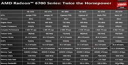
Source: PCinLife
Add your own comment

245 Comments on AMD Radeon HD 6700 Series ''Barts'' Specs Sheet Surfaces

#151
pantherx12
erockerMy GT 240.. if you want it. If you don't want it, you get a sense of satisfaction spurred by common sense. :D
I'll take it man :laugh:
Posted on Reply
#152
cheezburger
erockerHe gets my GT 240 if it does have a 512-bit bus. That's a promise... and if he/she wants it. :)
no..even my aged 9600gt reference can kick its ass....i want your 5850 :D
Posted on Reply
#153
btarunr
Editor & Senior Moderator
Dj-ElectriCwait... HD6770 = 1280SP, HD6970 = oh god....
Antilles? Since we're still stuck at 40 nm, AMD won't go bruteforce with its high-end GPU. All it has to do is outperform the GeForce GTX 480 512 SP (including at EVGA SSC speeds), maintain lower voltages/fan-noise/temperatures, and AMD is set for a long time. NVIDIA won't go beyond enabling the remaining 32 CUDA cores on its GTX 480, GF100 is a fail GPU with thermals. So don't expect NVIDIA to build a bigger GPU than GF100 on the existing 40 nm process.

So, 1920 4-D stream processors (I'm beginning to doubt AMD will continue to call these "stream processors"), and 2 GB of memory over a 256-bit wide GDDR5 memory interface clocked at 6.40 GHz (1600 MHz), might just do the trick. No doubt 28 nm process will be ready by late Q1, early Q2 at TSMC, but NVIDIA surely won't make a GPU with higher transistor count than GF100 on it right away. So Cayman is going to have a very long stint.

So, 3840 cores on the Antilles. If AMD does decide to double Barts in the SIMD department for Cayman, you're looking at 5120 cores.
erockerMy GT 240.. if you want it. If you don't want it, you get a sense of satisfaction spurred by common sense. :D
Or, I'll decide your avatar for a month.
Posted on Reply
#154
pantherx12
cheezburgerno..even my aged 9600gt reference can kick its ass....i want your 5850 :D
Use it as a dedicated phsyx card, pow!
Posted on Reply
#155
bear jesus
:laugh: an interesting turn of topic betting hardware on hardware, although i geuss it makes sense here :p
Posted on Reply
#156
erocker
*
btarunrOr, I'll decide your avatar for a month.
Well, if that's the case (since I agree with you on the subject), I'll have to take the stance that I believe it will be a 384-bit bus. Yeah, that's it.. It will be 384-bit. If I'm wrong, send me the avatar of your choice. :laugh:
Posted on Reply
#157
yogurt_21
btarunrAntilles? Since we're still stuck at 40 nm, AMD won't go bruteforce with its high-end GPU. All it has to do is outperform the GeForce GTX 480 512 SP (including at EVGA SSC speeds), maintain lower voltages/fan-noise/temperatures, and AMD is set for a long time. NVIDIA won't go beyond enabling the remaining 32 CUDA cores on its GTX 480, GF100 is a fail GPU with thermals. So don't expect NVIDIA to build a bigger GPU than GF100 on the existing 40 nm process.

So, 1920 4-D stream processors (I'm beginning to doubt AMD will continue to call these "stream processors"), and 2 GB of memory over a 256-bit wide GDDR5 memory interface clocked at 6.40 GHz (1600 MHz), might just do the trick. No doubt 28 nm process will be ready by late Q1, early Q2 at TSMC, but NVIDIA surely won't make a GPU with higher transistor count than GF100 on it right away. So Cayman is going to have a very long stint.

So, 3840 cores on the Antilles. If AMD does decide to double Barts in the SIMD department for Cayman, you're looking at 5120 cores.


Or, I'll decide your avatar for a month.
beyond the 512sp gtx480 there still is the dual gf104 rumor to contend with. ANd that will be a much more powerful card.
Posted on Reply
#158
cheezburger
pantherx12Use it as a dedicated phsyx card, pow!
not until i get his 5850 first :D then i'll trade my 9600gt to him for GT240 for physx :D
btarunrAntilles? Since we're still stuck at 40 nm, AMD won't go bruteforce with its high-end GPU. All it has to do is outperform the GeForce GTX 480 512 SP (including at EVGA SSC speeds), maintain lower voltages/fan-noise/temperatures, and AMD is set for a long time. NVIDIA won't go beyond enabling the remaining 32 CUDA cores on its GTX 480, GF100 is a fail GPU with thermals. So don't expect NVIDIA to build a bigger GPU than GF100 on the existing 40 nm process.

So, 1920 4-D stream processors (I'm beginning to doubt AMD will continue to call these "stream processors"), and 2 GB of memory over a 256-bit wide GDDR5 memory interface clocked at 6.40 GHz (1600 MHz), might just do the trick. No doubt 28 nm process will be ready by late Q1, early Q2 at TSMC, but NVIDIA surely won't make a GPU with higher transistor count than GF100 on it right away. So Cayman is going to have a very long stint.

So, 3840 cores on the Antilles. If AMD does decide to double Barts in the SIMD department for Cayman, you're looking at 5120 cores.
i don't see there's any point adding ridiculous number of shader on exist 40nm fab..based on my previous calculation if cayman is double of barts even except rops/bus increase as you were mention it will turn out to be like below if the spec is 2560:128:32 and 256bit bus

shader die space in cypress is 60% and 4D shader is 80% of 5D shader in size and SIMD controller and TMU took about 15% then here will be 2(334x 0.6 x0.8)+2(334x0.15)+334x0.25 = 320.64 + 100.2 +83.5 = 504.34mm^2 + hard wiring = 510mm^2

that is huge die and such 510mm^2 only has 32 rops????and i don't see any reason why we'd need 640ALU for? folding@home?
and you expect a 510mm^2 chip using a narrow 256bit bus on it?

if the shader turn out to be 5120(1280ALU) then the die size will be:

4(334x 0.6 x0.8)+4(334x0.15)+334x0.25 = 641.28 + 200.4 + 83.5 = 925.18mm^2 + hard wiring = 940mm^2......

shader like this are pointless if you don't have more rops to push it. like g92 was bottleneck by its 16 rop while it had 128 ALU. and now cayman that has 1280 ALU but 32 rops....that is a big joke...

if the specification turn out to be 1920:96:64 512bit story will be vastly different from above

1.5(334x0.6x0.8)+1.5(334x0.15)+2(334x0.25) = 240.48 + 75.15 + 167 = 482.64mm^2 + hard wiring = 484mm^2

480ALU is what we need in existed 40nm..no go further....
Posted on Reply
#159
btarunr
Editor & Senior Moderator
yogurt_21beyond the 512sp gtx480 there still is the dual gf104 rumor to contend with. ANd that will be a much more powerful card.
Correct, GeForce GTX 49x and GeForce GTX 475 (single GF104, 384 SP, high-clocks, 2 GB?, 4-way SLI support). At best, the GTX 49x might be competitive with the HD 5970, but if a single Cayman XT performs on par with HD 5970, there's little scope for GTX 49x.

GTX 475 is aimed at Barts XT.
Posted on Reply
#160
Unregistered
erockerHe gets my GT 240 if it does have a 512-bit bus. That's a promise... and if he/she wants it. :)
so can i join the bet? i really need that GT240 hahahaa:(
Posted on Edit | Reply
#161
AsRock
TPU addict
Dj-ElectriCwait... HD6770 = $300?, HD6970 = oh god....
:confused:
Posted on Reply
#162
JATownes
The Lurker
IDK if I like the bet. erocker without a Knight Rider avy would make me sad. Maybe just make him have a avy of Michael Knight :D

Posted on Reply
#163
wolf
Performance Enthusiast
cheezburgerthen bring some evidence to prove me wrong :D
or you could bring some evidence to prove yourself right :laugh: as oppose to the fruit of your imagination :)

I enjoy reading it and all, and if you seculate enough, some part of what you say is bound to be right, it's like flipping a coin.
Posted on Reply
#164
cheezburger
wolfor you could bring some evidence to prove yourself right :laugh: as oppose to the fruit of your imagination :)

I enjoy reading it and all, and if you seculate enough, some part of what you say is bound to be right, it's like flipping a coin.
well first i was confused by the media about the spec of barts that suppose to be 960shader(240ALU):48TMU:32rops but later it turn out to be whistler's spec(which higher than barts and performs between barts and hamlock). the roadmap suggest that cayman is double of 960:48:32 = 1920:96:64 with 512bit bus while whistler is 1280:64:32 and barts is 960:48:32. which that 1280:64:32 on barts was suppose to be whistler that was going to replace cypress and barts just mid range line. and whistler is different design rather than cut down version of cayman. but now amd just confuse people more and some sort of rename camouflage mix in just make the whole thing more...confuse..... chiphell were use either whistler or barts core during the benchmark i'm sure of it...


code name of amd's hd 6000 line

Antilles (6970~6990???)
Cayman (6850/6870~6950/6970???)
Whistler (???~6850/6870???)
Barts (6750~6770??)
blackcombs
Turks
Caicos
Posted on Reply
#165
erocker
*
Whistler? What the heck are you talking about? Show me some info on it? You are making less and less sense. :ohwell:
Posted on Reply
#166
bear jesus
cheezburgerwell first i was confused by the media about the spec of barts that suppose to be 960shader(240ALU):48TMU:32rops but later it turn out to be whistler's spec(which higher than barts and performs between barts and hamlock). the roadmap suggest that cayman is double of 960:48:32 = 1920:96:64 with 512bit bus while whistler is 1280:64:32 and barts is 960:48:32. which that 1280:64:32 on barts was suppose to be whistler that was going to replace cypress and barts just mid range line. and whistler is different design rather than cut down version of cayman. but now amd just confuse people more and some sort of rename camouflage mix in just make the whole thing more...confuse..... chiphell were use either whistler or barts core during the benchmark i'm sure of it...


code name of amd's hd 6000 line

Antilles (6970~6990???)
Cayman (6850/6870~6950/6970???)
Whistler (???~6850/6870???)
Barts (6750~6770??)
blackcombs
Turks
Caicos
:laugh: that confused me, but i blame the fact that it is 4:20am here in britland.

*edit*
erockerWhistler? What the heck are you talking about? Show me some info on it? You are making less and less sense. :ohwell:
I'm glad it is not just me is who is confused by that post :laugh:
Posted on Reply
#167
cheezburger
erockerWhistler? What the heck are you talking about? Show me some info on it? You are making less and less sense. :ohwell:
en.wikipedia.org/wiki/Northern_Islands_%28GPU_family%29

wiki may seem to be unreliable in some case (like comparison of graphic processing unit.) but this part has been protected under the community so i'm sure that article is real and it hasn't change since june/july.

wccftech.com/2010/08/27/upcoming-ati-hd-6000-series-codenames-revealed-catalyst-108/
www.nordichardware.com/news/69-cpu--chipset/40932-radeon-hd-6000-product-names-revealed-in-catalyst-108.html

this also prove its existence
Posted on Reply
#168
erocker
*
Whistler is a lower end card coming out next year. Below Barts.
Posted on Reply
#169
bear jesus
cheezburgeren.wikipedia.org/wiki/Northern_Islands_%28GPU_family%29

wiki may seem to be unreliable in some case (like comparison of graphic processing unit.) but this part has been protected under the community so i'm sure that article is real and it hasn't change since june/july.
Wiki is ONLY useful when he information shows a reliable source and none of the names have a source, i would assume they were sourced from the names within the drivers but i have never seen any numbers (supposed leaks or otherwise) of anything other than cayman and barts so i don't have a clue.

*edit*
erockerWhistler is a lower end card coming out next year. Below Barts.
Then i may have seen the picture of that assuming it was the small passive card, i can't remember the name as its too late/early here, i should be asleep.
Posted on Reply
#170
cheezburger
erockerWhistler is a lower end card coming out next year. Below Barts.
we don't know...if there's anything other than barts that's visible it will be cayman and caico but both of them are still myth-like.... we aint really know if these barts spec are real or belong to whistler or even blackcombs. which it is all unknown. even these prototype card from chiphell was merely just change the cooler but PCB is still barts...(or something idk)

gees...amd is acting like JJ Abrams as time goes.....
bear jesusWiki is ONLY useful when he information shows a reliable source and none of the names have a source, i would assume they were sourced from the names within the drivers but i have never seen any numbers (supposed leaks or otherwise) of anything other than cayman and barts so i don't have a clue.
actually everything in wiki are reliable except some fanboism controversy place like product comparison that's relate to spec of purely speculation. but when source come out it will be protect by community and these fanboi will go nowhere.
Posted on Reply
#171
erocker
*
Yet we're so darn sure Cayman will be 512 bit. It's not. This year there will be Barts, then Cayman then the dual GPU card. One of those names in the list could be for a different dual GPU card as well.
Posted on Reply
#172
cheezburger
erockerYet we're so darn sure Cayman will be 512 bit. It's not. This year there will be Barts, then Cayman then the dual GPU card. One of those names in the list could be for a different dual GPU card as well.
then where you going to put antilles if cayman is dual gpu? again we don't know yeah. that 512bit is just sarcastic reply on these people would damn believe 32rops + 256bit bus are just enough or like comment of "oh i couldn't even fill out my 4870's potential why get a powerful card anyway and most of game are ported so we just need a cheap card that needed!!". seriously technology is keep forward even you don't need it. and technology is all about performance that not what average people needs or about efficiency. (except iphone/ipad....) average people don't think/act as elite and they can't be trust.

technology is progress as ground breaking/brutal force(new technology/architecture)=> tweak,efficient redesign(reconfigure/die shrink)=>upward and push further performance with brutal force again. that is what moore's law about and these average consumer are about to destroy it. however hd 6000 will be just as what moore's law predict and all IC industry will follow until the end of humanity! that won't change forever.

moore's law and technology only serve elite, not average joe.
Posted on Reply
#173
erocker
*
cheezburgerthen where you going to put antilles if cayman is dual gpu?
Antilles is above cayman... Just like 5870-->5970. The way things are going Antilles is a dual Cayman (be it XT or Pro) GPU card. Perhaps they'll make a dual Barts GPU card as well. To the rest of your post.. Blah blah, heard it before. :cool:
Posted on Reply
#174
Unregistered
erockerWell, if that's the case (since I agree with you on the subject), I'll have to take the stance that I believe it will be a 384-bit bus. Yeah, that's it.. It will be 384-bit. If I'm wrong, send me the avatar of your choice. :laugh:
then i will betting 256bit bus with high speed GDDR5
#175
bear jesus
wahdangunthen i will betting 256bit bus with high speed GDDR5
I'm sure i read somewhere that hynix developed 1750mhz/7ghz effective gddr5 that was supposed to be in use/avalible by the end of this year, if that's right i'm sure that something at 5ghz or above would give more than enough bandwith on a 256bit bus on a top end chip.
Posted on Reply
Add your own comment
Apr 17th, 2024 20:32 EDT change timezone

New Forum Posts

Popular Reviews

Controversial News Posts