Tuesday, October 19th 2010

AMD Radeon HD 6800 Series Specifications Leaked
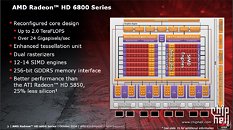
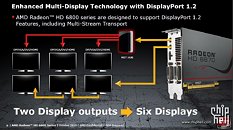
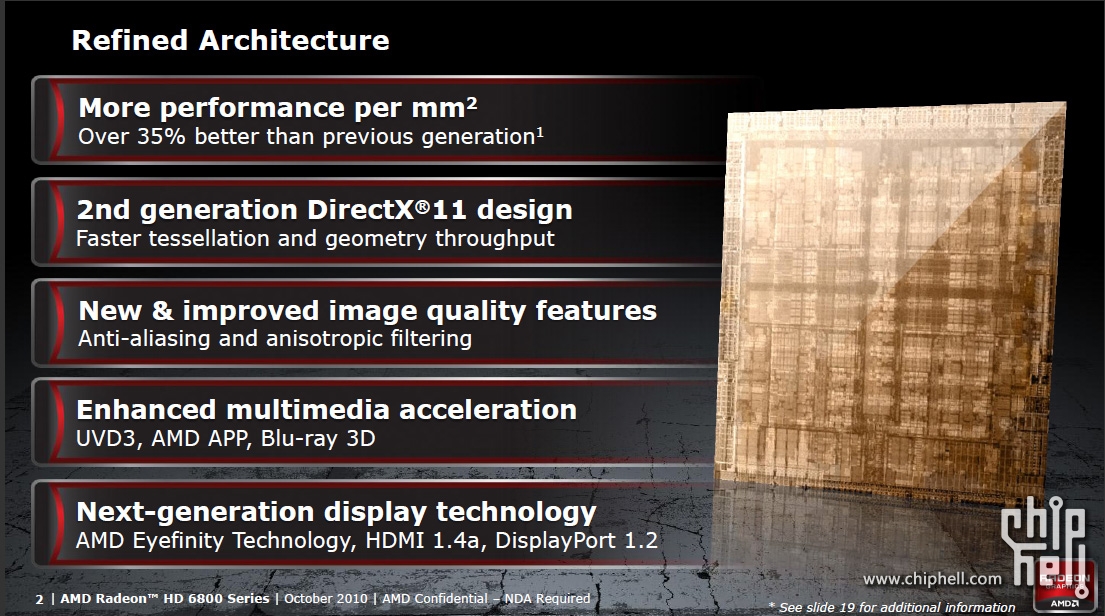
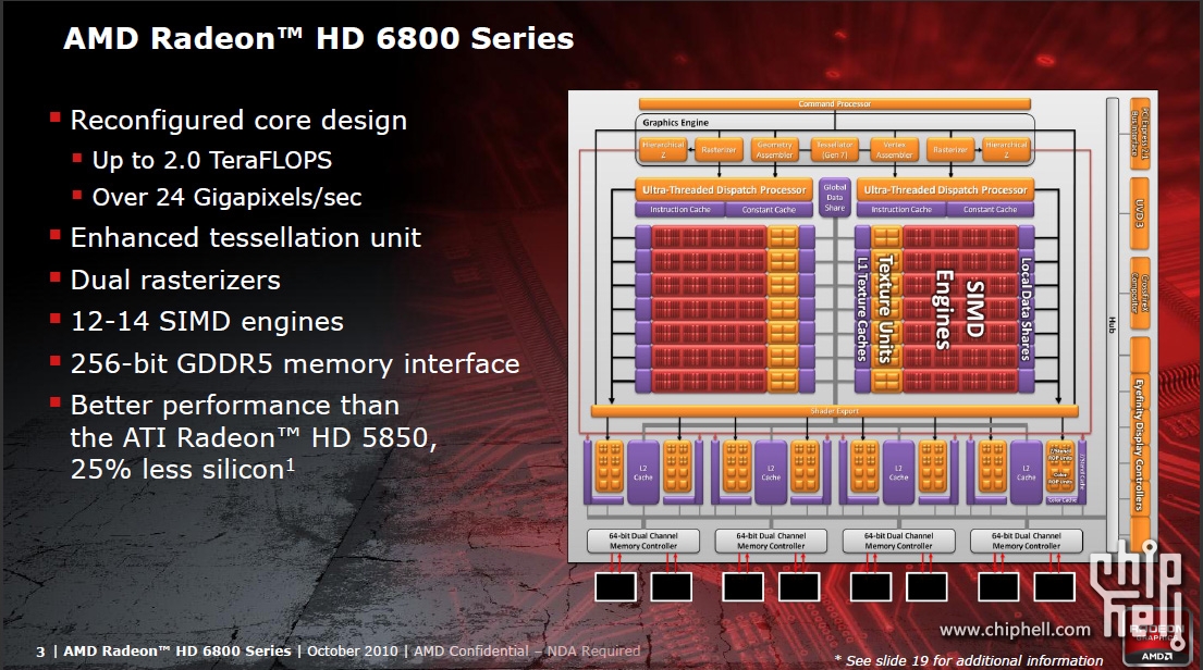
Specifications of the upcoming Radeon HD 6800 series GPUs have already been doing rounds for the last couple of days, and ChipHell.com finally managed to leak an alleged press-deck of the HD 6800 series that discloses the GPUs' specifications and some key features that AMD will introduce with this generation. What can be said looking at the slides is that AMD seems to have stepped up performance/die-size big time (up to 35% increase in performance per mm²), with some reconfiguring of key components. It also redesigned the GPUs to have up to 100% increase in tessellation performance, new image-quality enhancements, a new video acceleration engine (UVD 3), and a redesigned display IO with 2nd Gen. Eyefinity technology that can let users of standard variants drive up to six displays with a single card.
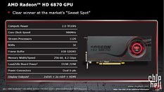
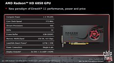
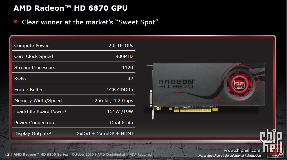
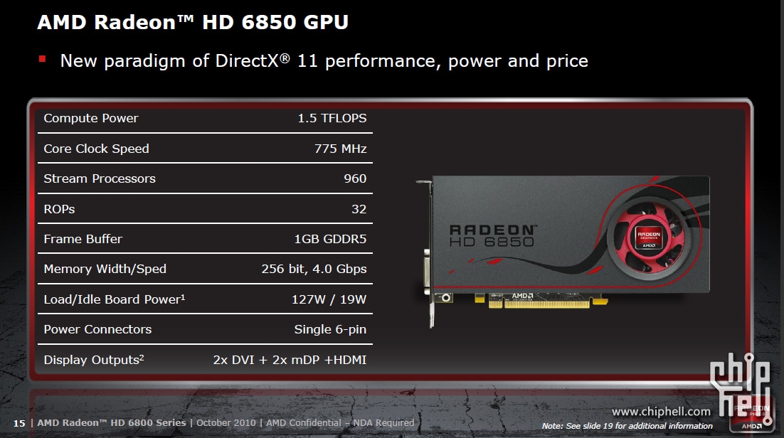
Specifications of the HD 6870 are: 1120 stream processors, 32 ROPs, 56 TMUs, 256-bit GDDR5 memory interface holding 1 GB, clock speeds of 900/1050(4200) MHz core/memory(effective), and idle/max board power of 19W/151W. For the HD 6850, it's 960 stream processors, 32 ROPs, 48 TMUs, 256-bit GDDR5 memory interface holding 1 GB, clock speeds of 775/1000(4000) MHz, idle/max board power of 19W/127W.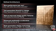
Source:
ChipHell
Specifications of the HD 6870 are: 1120 stream processors, 32 ROPs, 56 TMUs, 256-bit GDDR5 memory interface holding 1 GB, clock speeds of 900/1050(4200) MHz core/memory(effective), and idle/max board power of 19W/151W. For the HD 6850, it's 960 stream processors, 32 ROPs, 48 TMUs, 256-bit GDDR5 memory interface holding 1 GB, clock speeds of 775/1000(4000) MHz, idle/max board power of 19W/127W.

107 Comments on AMD Radeon HD 6800 Series Specifications Leaked
maybe some crossfire improvements too?
It's still specs, let see how far it improve over HD5870 and HD5850. :):toast:
I do not see 5870/5850 being obsoleted...the whole renaming and such will keep 5850/5870 value up.
Uploaded with ImageShack.us
Uploaded with ImageShack.us
forums.overclockers.com.au/showpost.php?p=12435812&postcount=1981
The 460 (768/1GB) is average 25% ish slower than the 6850/6870....even on games like metro 2033 that have tessellation. The 460 is doomed.
Slide says 12-14 SIMD engines, which MUST be 5-D(960/12=???:laugh:), shows seperate tesselator, etc...confirms 100% increase...ugh...this is exactly what i expected.
The 6850/6870 are to replace the 5770 performance bracket and to take on the Nvidia 460...which it does.
and
Got these from the link provided in post #9 of this topic.
What they have done to get the increase in performance is two set-up engines, seperating the die into two, and making like a real dual-core gpu, with each side of the dualcore having thier own tesselation engine. This way they can literally double the gpu usage(needed, based on my own experience with cypress, and poor Crossfire scaling exposing less than 60% gpu usage per card)
See, I know that they have issues keeping shaders filled, and that would perfectly fix that, and also explains the higher geometry throughput.
This is just a simple refresh.
If it WAS 4-D, then 800 shaders should basically double the performance of the previous gen, but this is not the case(ie, 6870 would be faster than 5870). I mean, I may be wrong, but I highly doubt they could also do this as stay pin-compatible with cypress...it would require a different power layout for the socket, IMHO. 4D would also require the set-up engine change, but I do not think we'd have SIMDs with 80 units any more.
Look at the slides. On the fourth they have shown a legend map of the die and you can see the 14 SIMDs. Each of them consists of 5 Texture units and if you look carefully, you can see that you have 4 texture cores in each TU, which hold the SPs. So if we say that the SPs are marked with "x", then x*4*5*14=1120 and that means that x = 4
Edit: I am guessing the 6850 has two SIMDS disabled, which would look like 4SPs*4TCs*5TU*12SIMDS=960SPs
I've blown up that pic you refer to as large as possible, and do not see anything to indicate what you are saying. Keep in mind, my 30-inch does a good job of displaying enlarged images.
Time will tell though...a short wait is all that is left.
Funny, now, many said the cards were going to launch today, and I said no(I actually said I doubt it possible because of constraints within memory production). Look...no real launch today...just some pictures...
Strangely enough, i thought it was more ... Must have confuse it with some other card, i guess.
And there's the source of my cursor corruption too.
Buggalugs, I have been running one monitor for some time now, as i RMA'ed one card a bit over two weeks ago. My idle clocks are 400/900. UVD clocks are 600/1250, and full speed is 900/1250.