Friday, December 17th 2010

EVGA P67 Classified Motherboard Looks Ferocious

EVGA unveiled its next enthusiast-grade motherboard, the P67 Classified. The board is designed for upcoming "Sandy Bridge" processors from Intel in the LGA1155 package, and uses the Intel P67 Express chipset. EVGA's main design goes seem to be: 1. giving the processor a strong VRM that helps with overclocking; and 2. to expand the board's PCI-Express resources using an nForce 200 bridge chip. The CPU is powered by a 12-phase VRM that draws power from two 8-pin EPS connectors. Knowing EVGA, the CPU socket is of premium-grade, with higher gold content on the pins. The four DDR3 DIMM slots are powered by a 3-phase VRM. The main ATX power connector is angled for better aesthetics.

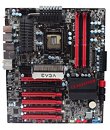
Expansion slots include six PCI-Express 2.0 x16 (electrical x16/x8;x1;x16/x8;x8;x16/x8;x8), making the board capable for 4-way SLI. A single PCI-E x1 is tucked away on top. Connectivity includes two internal SATA 6 Gb/s, four internal SATA 3 Gb/s, two front-panel and two rear-panel USB 3.0, 8-channel HD audio, two gigabit Ethernet controllers, FireWire, and eSATA. The board supports a plethora of overclocker-friendly technologies, including EVGA's EV-Bot module. One can expect more information once Intel's upcoming processors are out.
Add your own comment

49 Comments on EVGA P67 Classified Motherboard Looks Ferocious

#26
HillBeast
newtekie1The NF-200 does more than just PCI-E bandwidth expander, it is a bridge chip that takes 16 PCI-E lanes and converts them to 32 lanes. PCI 3.0 will not make a difference with the current or the next few GPU generations.

The PLX chips don't, AFAIK, have much lower TDPs compared to NF-200 and using the NF-200 nets you Tri-SLi support as well, so it is a no brainer why it was used here. The heatsink on this board is cooling the southbridge and the nf-200, and chances are the southbridge is why it is so big, not the nf-200.
I know what it does. I had a 9800GX2. And as for PCI-e 3.0 not making a difference, isn't it better to have that functionality for future proofing rather than cut it out completely? That means that super duper low end motherboards with a single GPU will have higher bandwidth capabilities than this super duper high end motherboard, and all because NVIDIA need to hurry up and make a new chipset.

I know the PLX chips don't do SLI,but I wasn't saying they should use that, I was more saying those chips use less power than the NF200, and the NF200 would be a 65nm or maybe 90nm chip. NVIDIA are now making 40nm chips. Why can't they die shrink it. That would probably reduce the TDP by 75% and as a result the cooling wouldn't need to be so extravagant.

Also there is a separate heatsink for the NF200 and the southbridge. They don't share a heatsink.
Posted on Reply
#27
nINJAkECIL
enlighten me plz.
i thought ever since p55(lga 1156),intel is moved the southbridge to cpu,and we get PCH for a change.
if so,why'd u guys talk about southbridge heatsink?
i'm sure the heatsinks are for vrm area,pch and nf200.
cmiiw
Posted on Reply
#28
hat
Enthusiast
newtekie1As I said the issue with your E2140 is probably that at anything above 266FSB these lower end processors have huge FSB holes. Both my E3200 and E2180 don't work at 333FSB but do work at higher FSB speeds.
We'll find out soon when my new power supply arrives. I'll play with it more then.
Posted on Reply
#29
HillBeast
nINJAkECILi'm sure the heatsinks are for vrm area,pch and nf200.
cmiiw
They are. The top two will be VRMs (obviously), the middle one will most likely be NF200, and the bottom one is the PCH.
Posted on Reply
#30
Zubasa
nINJAkECILenlighten me plz.
i thought ever since p55(lga 1156),intel is moved the southbridge to cpu,and we get PCH for a change.
if so,why'd u guys talk about southbridge heatsink?
i'm sure the heatsinks are for vrm area,pch and nf200.
cmiiw
They moved the northbridge to the CPU.
Posted on Reply
#31
Arctucas
PCIex1 slot is useless and it appears one would need to very careful with a card in the top x16 slot due to eVGA's continued ignorant cooler placement.
Posted on Reply
#32
Unregistered
Currently running a x58 Classified, ok for what i paid at the time, overpriced if you're paying over $300, but my next motherboard will be microATX and case, don't need SLI and only a few extra slots will be sufficient, bought into the SLI crap and up to now still haven't seen the need for it.

Asus boards are no better, same marketing crap with features you don't need. New Gigabyte boards with new color scheme however are looking rather tasty, microATX and I'm sold. www.youtube.com/watch?v=Bvg9Qs5cufY
Posted on Edit | Reply
#33
newtekie1
Semi-Retired Folder
CDdude55But isn't that what it would do then?, if it's adding extra lanes then you're getting more data throughput hence extra bandwidth. I thought it's sole purpose was in fact to add more lanes for boards with multiple PCI-E slots to gain more bandwidth that the chipset couldn't provide and nothing more.

But if there is more to it, i'd like to know.
Increasing the number of lanes is more specific than simply increasing the bandwidth. Going from PCI-E 1.0 to PCI-E 2.0 was a bandwidth increase, converting 16 lanes into 32 lanes allows for more devices or more lanes per device.
HillBeastI know what it does. I had a 9800GX2. And as for PCI-e 3.0 not making a difference, isn't it better to have that functionality for future proofing rather than cut it out completely? That means that super duper low end motherboards with a single GPU will have higher bandwidth capabilities than this super duper high end motherboard, and all because NVIDIA need to hurry up and make a new chipset.

I know the PLX chips don't do SLI,but I wasn't saying they should use that, I was more saying those chips use less power than the NF200, and the NF200 would be a 65nm or maybe 90nm chip. NVIDIA are now making 40nm chips. Why can't they die shrink it. That would probably reduce the TDP by 75% and as a result the cooling wouldn't need to be so extravagant.

Also there is a separate heatsink for the NF200 and the southbridge. They don't share a heatsink.
You make some assumption, possible because you don't have all the information. AFAIK, P67 only gives out 16 PCI-E 3.0 lanes(from the CPU). It is more than likely that the single black slot is the 3.0 slot, gaining all the benefits of 3.0. The other slots are run off the 2.0 lanes provided by the rest of the chipset.

As for the TDP and die shrink issue, I believe the NF200 is currently on 55nm, and the move to 40nm isn't as simple as smiply shrinking the die, the chip would have to be redesigned. And as I said, the PLX chips don't have much lower TDP than the NF200, and still require a heatsink themselves.

And that big heatsink you highlighted is not what is required to cool a single NF200 chip, so don't kid yourself in assuming that entire heatsink is dedicated to an NF200 chip. If you've seen some of the other heatsinks that have been used to cool the NF200 in the past you would know that big of a heatsink isn't required. It could easily share the southbridge heatsink you highlighted without problem.
Posted on Reply
#34
CDdude55
Crazy 4 TPU!!!
newtekie1Increasing the number of lanes is more specific than simply increasing the bandwidth. Going from PCI-E 1.0 to PCI-E 2.0 was a bandwidth increase, converting 16 lanes into 32 lanes allows for more devices or more lanes per device.
I know PCI-E 1.0/1.1--2.0/2.1--3.0 are bandwidth increases/incremental improvements to the PCI-E standard, but im still not clear on this lol, what would be the advantage exactly for throwing on a PLX or NF-200 chip?, it's increasing the number of lanes to be taken advantage of by what exactly?,
Posted on Reply
#35
HillBeast
newtekie1You make some assumption, possible because you don't have all the information. AFAIK, P67 only gives out 16 PCI-E 3.0 lanes(from the CPU). It is more than likely that the single black slot is the 3.0 slot, gaining all the benefits of 3.0. The other slots are run off the 2.0 lanes provided by the rest of the chipset.
You serious? I know EVGA aren't too bright, but you honestly think they'd bottleneck the graphics cards that much by making them go through the NF200, then the southbridge, then to the CPU? That's just stupidity. You would never do that. It was okay back when they had QPI and all that, but DMI has nowhere near the bandwidth of QPI. Don't tell me that they may have redesigned DMI in this generation to give a higher bandwidth because there is no way it could provide THAT much of a difference with such a low pin count in the CPU.
newtekie1As for the TDP and die shrink issue, I believe the NF200 is currently on 55nm, and the move to 40nm isn't as simple as smiply shrinking the die, the chip would have to be redesigned. And as I said, the PLX chips don't have much lower TDP than the NF200, and still require a heatsink themselves.
NF200 on a nForce 780i motherboard


NF200 on a GeForce 9800GX2


NF200 on a GTX295


NF200 on a X58 Classified


Doesn't look like it's gotten any smaller, and considering when it was first made, they were only on 65nm... dude, it's not 55nm. It's 65nm or 90nm. It needs a die shrink. I don't care how they do it, they just need to do it.
newtekie1And that big heatsink you highlighted is not what is required to cool a single NF200 chip, so don't kid yourself in assuming that entire heatsink is dedicated to an NF200 chip. If you've seen some of the other heatsinks that have been used to cool the NF200 in the past you would know that big of a heatsink isn't required. It could easily share the southbridge heatsink you highlighted without problem.
Oh right I see. Motherboard manufacturers just love putting giant coolers in the middle of the motherboard that cool nothing, don't they...

What else would it be for, and don't say the southbridge because then that would be by far the STUPIDEST place to put a southbridge. It should go in the corner with the SATA and USB connectors.
Posted on Reply
#36
newtekie1
Semi-Retired Folder
CDdude55I know PCI-E 1.0/1.1--2.0/2.1--3.0 are bandwidth increases/incremental improvements to the PCI-E standard, but im still not clear on this lol, what would be the advantage exactly for throwing on a PLX or NF-200 chip?, it's increasing the number of lanes to be taken advantage of by what exactly?,
Ok, using the standard 16 lanes provided by the chipset. You can split that into two x8 slots without any noticeable performance degradation. But splitting it into four x4 slots will show performance issues.

The 32 lanes provided by NF200 means you can have four x8 slots for graphics cards for up to Quad-SLi/Crossfire.
HillBeastYou serious? I know EVGA aren't too bright, but you honestly think they'd bottleneck the graphics cards that much by making them go through the NF200, then the southbridge, then to the CPU? That's just stupidity. You would never do that. It was okay back when they had QPI and all that, but DMI has nowhere near the bandwidth of QPI. Don't tell me that they may have redesigned DMI in this generation to give a higher bandwidth because there is no way it could provide THAT much of a difference with such a low pin count in the CPU.
It seems to be more of an poor design choice on Intels part, only giving 16 lanes coming from the Northbridge/CPU actually.
HillBeastNF200 on a nForce 780i motherboard

news.softpedia.com/images/news2/Nvidia-039-s-New-780i-Chipset-Previewed-2.jpg

NF200 on a GeForce 9800GX2

images.bit-tech.net/content_images/2008/03/xfx_geforce_9800_gx2_600m_1gb_graphics_card/h1.jpg

NF200 on a GTX295

i40.tinypic.com/wgpwn9.jpg

NF200 on a X58 Classified

www.overclockerstech.com/images/reviews/Lvcoyote/evgax58/evgax5829.jpg

Doesn't look like it's gotten any smaller, and considering when it was first made, they were only on 65nm... dude, it's not 55nm. It's 65nm or 90nm. It needs a die shrink. I don't care how they do it, they just need to do it.
It might not be smaller, but it doesn't necessarily need a die shrink either. Look at the die, it is pretty damn small, and so it its TDP.
HillBeastOh right I see. Motherboard manufacturers just love putting giant coolers in the middle of the motherboard that cool nothing, don't they...

What else would it be for, and don't say the southbridge because then that would be by far the STUPIDEST place to put a southbridge. It should go in the corner with the SATA and USB connectors.
I know, it would be unheard of for motherboard manufacturers to put things in that location that aren't really needed just for looks.

GIGABYTE GA-P55A-UD4P LGA 1156 Intel P55 SATA 6Gb/...

EVGA P55 SLI 132-LF-E655-KR LGA1156 Intel P55 ATX ...

MSI P55-GD80 LGA 1156 Intel P55 ATX Intel Motherbo...

GIGABYTE GA-P55-UD6 LGA 1156 Intel P55 ATX Intel M...

ASUS Maximus III Formula LGA 1156 Intel P55 ATX In...

And if you want an idea of just how little it takes to cool an NF200 look at the eVGA 750i board. EVGA 122-YW-E173-TR LGA 775 NVIDIA nForce 750i SLI...

It has a little heatsink cooling the southbridge and the NF200. It doesn't have a huge TDP like you seem to think. Hell they did the same thing with my P55 FTW 200, sticking a huge heatsink on the NF200, and the heatsink never goes above ambient. It is just way to big, and put there for looks more than necessity.
Posted on Reply
#37
sneekypeet
Retired Super Moderator
They are useless for direct heat transfer, but most are piped to the CPU power heatsinks as well. So while it doesn't cool anything directly, via the pipe they are adding cooling to an otherwise ugly spot on the mobo if left bare;)

GB helps cool the CPU phase
EVGA is a light, not a heatsink
MSI and ASUS fall in with the GB;)
Posted on Reply
#38
newtekie1
Semi-Retired Folder
sneekypeetThey are useless for direct heat transfer, but most are piped to the CPU power heatsinks as well. So while it doesn't cool anything directly, via the pipe they are adding cooling to an otherwise ugly spot on the mobo if left bare;)

GB helps cool the CPU phase
EVGA is a light, not a heatsink
MSI and ASUS fall in with the GB;)
Yes, EVGA's is a light. So it is not logical to think they would use an oversized heatsink for looks? NF200 doesn't need that big of a heatsink.
Posted on Reply
#39
HillBeast
newtekie1It might not be smaller, but it doesn't necessarily need a die shrink either. Look at the die, it is pretty damn small, and so it its TDP.
Just because it's small, doesn't mean they shouldn't save some money and make it smaller. It is a hot little chip. The one on my GX2 gave me all kinds of hell with it's heat, which was the killer of my GX2. I am not going to explain all the diagnosis I had to go through to figure it out because it took me months, but it WAS the NF200 causing me trouble with that thing.
newtekie1I know, it would be unheard of for motherboard manufacturers to put things in that location that aren't really needed just for looks.

GIGABYTE GA-P55A-UD4P LGA 1156 Intel P55 SATA 6Gb/...

EVGA P55 SLI 132-LF-E655-KR LGA1156 Intel P55 ATX ...

MSI P55-GD80 LGA 1156 Intel P55 ATX Intel Motherbo...

GIGABYTE GA-P55-UD6 LGA 1156 Intel P55 ATX Intel M...

ASUS Maximus III Formula LGA 1156 Intel P55 ATX In...
All of those motherboard either aren't heatsinks (the EVGA) or the are heatpiped to the VRMs, meaning your arguement is debunked. This motherboard doesn't have a heatpipe there. Are you seriously telling me EVGA woke up one morning and thought 'Hey that P67 board, know what it's missing? A heatsink for nothing. Let's just ram it on there. Nobody will care that it doesn't do anything. Nobody will complain it's a waste of money. Nah it's fine. Just do it to troll them'. No. EVGA are stupid, but not that stupid. Seriously, that is a heatsink for cooling something, and the only chips on the motherboard that need cooling are the NF200 and the southbridge. EVGA would NEVER be stupid enough to put the PCH between the CPU and the PCI-e cards, and the NF200 down in the corner.
newtekie1And if you want an idea of just how little it takes to cool an NF200 look at the eVGA 750i board. EVGA 122-YW-E173-TR LGA 775 NVIDIA nForce 750i SLI...

It has a little heatsink cooling the southbridge and the NF200. It doesn't have a huge TDP like you seem to think. Hell they did the same thing with my P55 FTW 200, sticking a huge heatsink on the NF200, and the heatsink never goes above ambient. It is just way to big, and put there for looks more than necessity.
So if it doesn't need a big heatsink, then what is that heatsink for. EVGA won't be putting a massive heatsink that isn't heatpiped into something that only cools a sticker.

Show me a motherboard that has a heatsink, not a little gizmo that lights up, but an actual heatsink, that does nothing.
Posted on Reply
#40
sneekypeet
Retired Super Moderator
newtekie1Yes, EVGA's is a light. So it is not logical to think they would use an oversized heatsink for looks? NF200 doesn't need that big of a heatsink.
funny my NF200 chip gets hot as balls, hence why the huge Cool-Pipe or water block add on;)
Posted on Reply
#41
sixthseven
for now, it's better to use x58 chipset I think... UD9 from gigabyte will be great.. It's a value highend gaming mobo..
Posted on Reply
#42
sneekypeet
Retired Super Moderator
sixthsevenUD9 from gigabyte will be great.. It's a value highend gaming mobo..
I hope UD9 and value aren't meant to go together;)
Posted on Reply
#43
sixthseven
sneekypeetI hope UD9 and value aren't meant to go together;)
well, it isn't expensive, is it ?:D
Posted on Reply
#45
Johnny87au
they went way over the top adding that many pcie for a SB mobo..
Posted on Reply
#46
newtekie1
Semi-Retired Folder
HillBeastJust because it's small, doesn't mean they shouldn't save some money and make it smaller. It is a hot little chip. The one on my GX2 gave me all kinds of hell with it's heat, which was the killer of my GX2. I am not going to explain all the diagnosis I had to go through to figure it out because it took me months, but it WAS the NF200 causing me trouble with that thing.


All of those motherboard either aren't heatsinks (the EVGA) or the are heatpiped to the VRMs, meaning your arguement is debunked. This motherboard doesn't have a heatpipe there. Are you seriously telling me EVGA woke up one morning and thought 'Hey that P67 board, know what it's missing? A heatsink for nothing. Let's just ram it on there. Nobody will care that it doesn't do anything. Nobody will complain it's a waste of money. Nah it's fine. Just do it to troll them'. No. EVGA are stupid, but not that stupid. Seriously, that is a heatsink for cooling something, and the only chips on the motherboard that need cooling are the NF200 and the southbridge. EVGA would NEVER be stupid enough to put the PCH between the CPU and the PCI-e cards, and the NF200 down in the corner.


So if it doesn't need a big heatsink, then what is that heatsink for. EVGA won't be putting a massive heatsink that isn't heatpiped into something that only cools a sticker.

Show me a motherboard that has a heatsink, not a little gizmo that lights up, but an actual heatsink, that does nothing.
Again, they did the same thing with the P55 FTW 200, the board I have, and the heatsink is never even warm to the touch. It is totally overkill for the NF200 under it, and done for nothing more than to make the motherboard look beefy. As I've said as well, there are other designs where the NF200 is sharing tiny flat heatsinks with the southbridge.
sneekypeetfunny my NF200 chip gets hot as balls, hence why the huge Cool-Pipe or water block add on;)
It probably does get hot, but not hot enough to require that big of a heatsink, and the PLX alternatives get just as hot.
Posted on Reply
#48
Johnny87au
johnnyfiiveASUS or GTFO.
:toast::nutkick::toast:
Posted on Reply
#49
Maban
Little update on this. Name changed to FTW and said to be releasing this month.
Posted on Reply
Add your own comment
Apr 25th, 2024 08:25 EDT change timezone

New Forum Posts

Popular Reviews

Controversial News Posts