Tuesday, October 16th 2012

Tesla K20 GPU Compute Processor Specifications Released
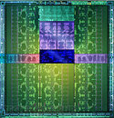
Specifications of NVIDIA's Tesla K20 GPU compute processor, which was launched way back in May, are finally disclosed. We've known since then that the K20 is based on NVIDIA's large GK110 GPU, a chip never used to power a GeForce graphics card, yet. Apparently, NVIDIA is leaving some room on the silicon that allows it to harvest it better. According to a specifications sheet compiled by Heise.de, Tesla K20 will feature 13 SMX units, compared to the 15 available on the GK110 silicon.
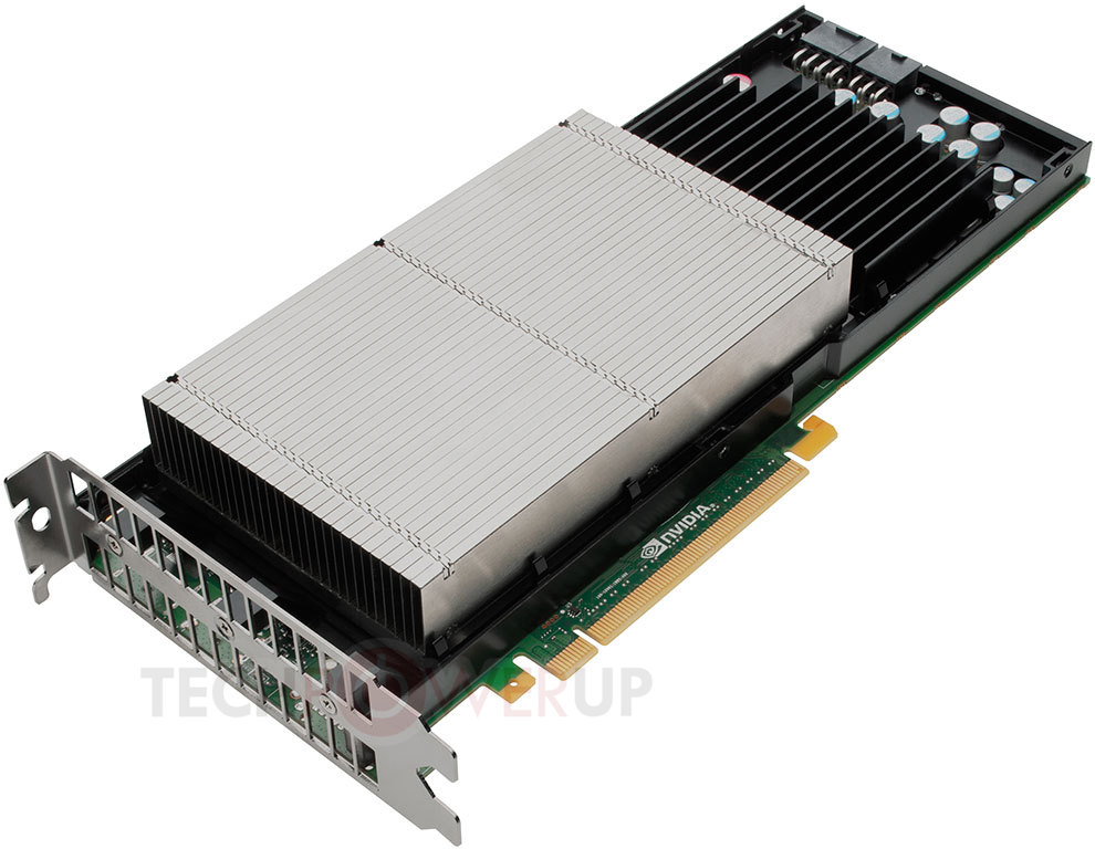
With 13 streaming multiprocessor (SMX) units, the K20 will be configured with 2,496 CUDA cores (as opposed to 2,880 physically present on the chip). The core will be clocked at 705 MHz, yielding single-precision floating point performance of 3.52 TFLOP/s, and double-precision floating point performance of 1.17 TFLOP/s. The card packs 5 GB of GDDR5 memory, with memory bandwidth of 200 GB/s. Dynamic parallelism, Hyper-Q, GPUDirect with RDMA are part of the new feature-set. The TDP of the GPU is rated at 225W, and understandably, it uses a combination of 6-pin and 8-pin PCI-Express power connectors. Built in the 28 nm process, the GK110 packs a whopping 7.1 billion transistors.
Source:
Heise.de
With 13 streaming multiprocessor (SMX) units, the K20 will be configured with 2,496 CUDA cores (as opposed to 2,880 physically present on the chip). The core will be clocked at 705 MHz, yielding single-precision floating point performance of 3.52 TFLOP/s, and double-precision floating point performance of 1.17 TFLOP/s. The card packs 5 GB of GDDR5 memory, with memory bandwidth of 200 GB/s. Dynamic parallelism, Hyper-Q, GPUDirect with RDMA are part of the new feature-set. The TDP of the GPU is rated at 225W, and understandably, it uses a combination of 6-pin and 8-pin PCI-Express power connectors. Built in the 28 nm process, the GK110 packs a whopping 7.1 billion transistors.

29 Comments on Tesla K20 GPU Compute Processor Specifications Released
The first Fermi Tesla's (M2050/M2070) out of the gate were basically GTX 470 spec. M2090 released more recently is pretty much a GTX 580.
Would be interesting to know whether these Tesla's are the same SKU's that ORNL are taking delivery of, or whether they are higher spec since Oak Ridge seemed to be the high profile launch customer.Any comparison probably depends on actual performance efficiencyrather than hypothetical. Unless you know what K20 brings to the table, a theoretical comparison is largely useless.
BTW: The original sitenow no longer features any specification
Nice peak.
I wish 20 PFOPS/s on next GPU option.:D
So you might want to check who runs the sites your linking to if you want to link to un-bias information.
It be like linking to sites/blog run by AMD employees to make a point or further a view point of a AMD product.
Just silly.
:roll:
That site is run by Mark Harris a Nvidia employee. Are you so naive that hes gonna post un-bias research link on his site/blog.
Nvidia would find a way to fire him in a second if he posted links to research papers that put Nvidia in a bad light.
It only took me 1 mouse click to findout he was a Nvidia employee. Come-on now. Whos trolling now ?
Atleast show both sides or attempt to so you wont seam like a Nvidia cheerleaderThats from a Oak Ridge National Labaratory along with University of Tennesse and University of Manchester in UK study.
58% is lower then 90% in DGEMM. Maybe Kepler GK100/110 has a 34% jump who knows but chip on the GTX 280 was only 34% in DGEMM.
What do i know tho. I would think Oak Ridge National Labaratory does since they use the darn things.;)
All I see here is a brief synopsis of Fermi
And of course, at no point did I make an AMD vs Nvidia comparison- quite the opposite in factGet back under your bridge Xzibitroll - I'm sick of having to explain simple compound sentences to you.
previous gen NVidia architecture calculates floating points by shader clock so the C2050 would be 1Tflop of single precision
C2050 is 515 GFlop/s in double precision so its only 58% as advertised.
Kepler would have to make up alot of ground in effeciency.
The point i was try'n to make was..
Pointing to a 90% effeciency of Tahiti in DGEMM as if its a bad thing, Especially from a site/blog of a Nvidia employee.
As compared to what ? Nvidias Fermi 58% effeciency in DGEMM ? That Nvidia employee doesnt have a link to that on his site. Wonder why ?
Even if Tahiti ran 58% it still be twice as fast in DGEMM compared to Fermi.
Given K20 is similar spec to W9000 and W8000 It would have to bring its efficiency up in such a comparison.
Maybe the K20 has better effeciency but when someone says hey look AMD can only do 90% when they fail to mention Nvidia only does 58% thats kind cheerleading to me.
We need to see Keplers DGEMM effeciency to see what % it is to its specs/as advertised.
:toast:
Update:
Nvidias marketing slides put DGEMM efficiency of K20 at 80% and Fermi at 60-65%. So if Oak Ridge National Laboratories put it 2% shy of 60% I would say the window would be 78-80% efficiency for K20. So we are more then likely going to see a draw between K20 & W9000 in DGEMM if the marketing slides of 80% effeciency are met.
Still, coming from someone who openly admits to lying, and up until recently didn't even know the difference between a 3D rendering card and a math co-processor, it's hardly surprising.Keep up with the straw man AMD vs Nvidia bullshit and the hypothetical numbers game. I'll stand by my preference for real world testing**By your reasoning the AMD FirePro W9000 (3.99 TF SP, 1 TF DP) should be four times faster than a Quadro 6000 (1 TF SP, 515 GF DP)...after all, numbers don't lie right?
No...
No...
No
This coming from the idiot who didnt even know who ran GPGPU.ORG
Mark Harris,
Chief Technologist, GPU Computing @ Nvidia
I thought we wanted hard numbers not marketing B.S.
Are you gonna link to Jen-Hsun Huang blog next so we can get nvidia links from there aswell :laugh:
In fact you are the one who introduced the Nvidia informationSo if anyone is treating marketing slides as fact...it's you.Site reports university research paper. Linked.
Troll trys to sidetrack by highlighting a non-issue to divert attention from the fact that their straw man argument is shown to garbage. Achievement unlocked !!!