Thursday, August 2nd 2018

NVIDIA GeForce GTX 1180 Bare PCB Pictured
Here are some of the first pictures of the bare printed circuit board (PCB) of NVIDIA's upcoming GeForce GTX 1180 graphics card (dubbed PG180), referred to by the person who originally posted them as "GTX 2080" (it seems the jury is still out on the nomenclature). The PCB looks hot from the press, with its SMT points and vias still exposed. The GT104 GPU traces hint at a package that's about the size of a GP104 or its precessors. It's wired to eight memory chips on three sides, confirming a 256-bit wide memory bus. Display outputs appear flexible, for either 2x DisplayPort + 2x HDMI, or 3x DisplayPort + 1x HDMI configurations.
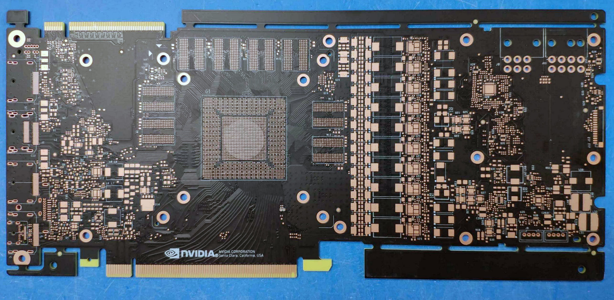
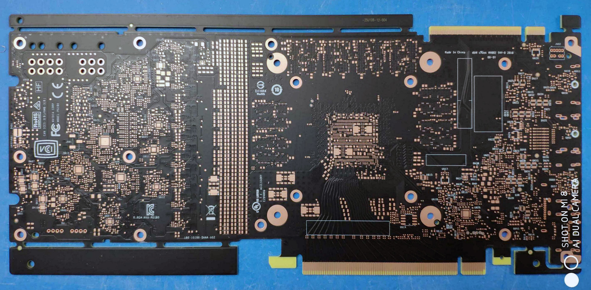
The VRM setup is surprisingly powerful for a card that's supposed to succeed the ~180W GeForce GTX 1080, which can make do with a single 8-pin PCIe power input. The card draws power from a combination of 6-pin and 8-pin PCIe power connectors. There is a purportedly 10-phase VCore side, which in all likelihood is a 5-phase setup with "dumb" phase-doubling; and similarly, a 2-phase memory power (which could again be doubled single-phase). The SLI-HB fingers also make way. There's a new connector that looks like a single SLI finger and an NVLink finger arranged side-by-side. NVIDIA still hasn't given up on multi-GPU. NVLink is a very broad interconnect, in terms of bandwidth. NVIDIA probably needs that for multi-GPU setups to work with not just high resolutions (4K, 5K, or even 8K), but also higher bit-depth, higher refresh-rates, HDR, and other exotic data. The reverse side doesn't have much action other than traces for the VRM controllers, phase doublers, and an unusually large bank of SMT capacitors (the kind seen on AMD PCBs with MCM GPUs).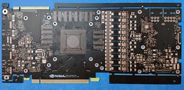

Sources:
Baidu Tieba, VideoCardz
The VRM setup is surprisingly powerful for a card that's supposed to succeed the ~180W GeForce GTX 1080, which can make do with a single 8-pin PCIe power input. The card draws power from a combination of 6-pin and 8-pin PCIe power connectors. There is a purportedly 10-phase VCore side, which in all likelihood is a 5-phase setup with "dumb" phase-doubling; and similarly, a 2-phase memory power (which could again be doubled single-phase). The SLI-HB fingers also make way. There's a new connector that looks like a single SLI finger and an NVLink finger arranged side-by-side. NVIDIA still hasn't given up on multi-GPU. NVLink is a very broad interconnect, in terms of bandwidth. NVIDIA probably needs that for multi-GPU setups to work with not just high resolutions (4K, 5K, or even 8K), but also higher bit-depth, higher refresh-rates, HDR, and other exotic data. The reverse side doesn't have much action other than traces for the VRM controllers, phase doublers, and an unusually large bank of SMT capacitors (the kind seen on AMD PCBs with MCM GPUs).
57 Comments on NVIDIA GeForce GTX 1180 Bare PCB Pictured
What I do know is that "GV102" and "GV104" was taped out before last summer, and that Nvidia is about to release a lineup of new GeForce cards which will be "Volta based". I don't know what product names and "architecture" names Nvidia will use for branding, and frankly I don't care.Many assume the RTX technology uses these. RTX is primarily designed for consumers.
Anyway, it's very common that Nvidia reduce or eliminate features on their lower models. Like GP102 reduces fp64 and removes fp16 support vs. GP102, along with a different memory controller, etc.
You may be right that Volta-based GPUs are being announced in a few weeks and, excepting the GV100 (with Tensor cores) are just 12nm rehashes of Pascal. We'll find out in due time.
I recommend reading the White paper from Nvidia, or some of the articles from Anandtech.
Especially page 10-12 from the white paper is an interesting read, some snippets:And so much more. I highly recommend reading it, since it's a good insight into what's going to trickle down to the consumers.
But as you are saying, TSMC "12nm FFN" is not any denser than 16nm at all, it's just a refinement.