Monday, July 6th 2020

Samsung Leads Semiconductor Paradigm Shift with New Material Discovery
Researchers at the Samsung Advanced Institute of Technology (SAIT) have unveiled the discovery of a new material, called amorphous boron nitride (a-BN), in collaboration with Ulsan National Institute of Science and Technology (UNIST) and the University of Cambridge. Published in the journal Nature, the study has the potential to accelerate the advent of the next generation of semiconductors.
Recently, SAIT has been working on the research and development of two-dimensional (2D) materials - crystalline materials with a single layer of atoms. Specifically, the institute has been working on the research and development of graphene, and has achieved groundbreaking research outcomes in this area such as the development of a new graphene transistor as well as a novel method of producing large-area, single-crystal wafer-scale graphene. In addition to researching and developing graphene, SAIT has been working to accelerate the material's commercialization.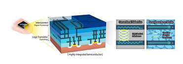 "To enhance the compatibility of graphene with silicon-based semiconductor processes, wafer-scale graphene growth on semiconductor substrates should be implemented at a temperature lower than 400°C." said Hyeon-Jin Shin, a graphene project leader and Principal Researcher at SAIT. "We are also continuously working to expand the applications of graphene beyond semiconductors."
2D Material Transformed - Amorphous Boron Nitride
The newly discovered material, called amorphous boron nitride (a-BN), consists of boron and nitrogen atoms with an amorphous molecule structure. While amorphous boron nitride is derived from white graphene, which includes boron and nitrogen atoms arranged in a hexagonal structure, the molecular structure of a-BN in fact makes it uniquely distinctive from white graphene.
Amorphous boron nitride has a best-in-class ultra-low dielectric constant of 1.78 with strong electrical and mechanical properties, and can be used as an interconnect isolation material to minimize electrical interference. It was also demonstrated that the material can be grown on a wafer scale at a low temperature of just 400°C. Thus, amorphous boron nitride is expected to be widely applied to semiconductors such as DRAM and NAND solutions, and especially in next generation memory solutions for large-scale servers.
"Recently, interest in 2D materials and the new materials derived from them has been increasing. However, there are still many challenges in applying the materials to existing semiconductor processes." said Seongjun Park, Vice President and Head of Inorganic Material Lab, SAIT. "We will continue to develop new materials to lead the semiconductor paradigm shift."
Timeline:
Recently, SAIT has been working on the research and development of two-dimensional (2D) materials - crystalline materials with a single layer of atoms. Specifically, the institute has been working on the research and development of graphene, and has achieved groundbreaking research outcomes in this area such as the development of a new graphene transistor as well as a novel method of producing large-area, single-crystal wafer-scale graphene. In addition to researching and developing graphene, SAIT has been working to accelerate the material's commercialization.

2D Material Transformed - Amorphous Boron Nitride
The newly discovered material, called amorphous boron nitride (a-BN), consists of boron and nitrogen atoms with an amorphous molecule structure. While amorphous boron nitride is derived from white graphene, which includes boron and nitrogen atoms arranged in a hexagonal structure, the molecular structure of a-BN in fact makes it uniquely distinctive from white graphene.
Amorphous boron nitride has a best-in-class ultra-low dielectric constant of 1.78 with strong electrical and mechanical properties, and can be used as an interconnect isolation material to minimize electrical interference. It was also demonstrated that the material can be grown on a wafer scale at a low temperature of just 400°C. Thus, amorphous boron nitride is expected to be widely applied to semiconductors such as DRAM and NAND solutions, and especially in next generation memory solutions for large-scale servers.
"Recently, interest in 2D materials and the new materials derived from them has been increasing. However, there are still many challenges in applying the materials to existing semiconductor processes." said Seongjun Park, Vice President and Head of Inorganic Material Lab, SAIT. "We will continue to develop new materials to lead the semiconductor paradigm shift."
Timeline:
- 2012: Graphene Barristor, a Triode Device with a Gate-Controlled Schottky Barrier (SAIT, published in Science)
- 2014: Wafer-Scale Growth of Single-Crystal Monolayer Graphene on Reusable Hydrogen-Terminated Germanium (SAIT and Sungkyunkwan University, published in Science)
- 2017: Realization of continuous Zachariasen carbon monolayer (SAIT and Sungkyunkwan University, published in Science Advances)
- 2020: Ultra-low dielectric constant amorphous boron nitride (SAIT, UNIST and University of Cambridge, published in Nature)
10 Comments on Samsung Leads Semiconductor Paradigm Shift with New Material Discovery
The only issue, of course, is how much this will cost to manufacture and how long the lead time to market will be. The fact that we don't have any type of graphene products in commercial production today suggests it will sadly be a long time before we see a-BN semiconductors in our PCs.
Reinventing new ways of using existing material is much cheaper than deploying new materials at the moment BUT a certain amount of the vast profits should go in to actually using these new material in manufacturing NOW.
When we cannot further develop our existing materials and have no new materials in manufacturing, progress will stop and it will then be an enormous time gap until any of these materials can be used if we don't already have them integrated in our manufacturing.
By using new material now we will have invented ways to integrate them cost effectively in to manufacturing by the time we really need them.
Most stock investors are only interested in short term profits and that is eroding the electronics industry in the way that the industry adapt to that way of doing business and sacrifices progress to obtain short term profits instead.
There should be two kind of stock, short and long term investment stock. If you invest in long term stock your part of the profit share will grow higher each year giving you much more of the profits in the end opose to other doing short term hit and run investments.
If the electro-chemical properties are to be believed, this could be a very big step forward in IC design as well as the potential for a replacement for standard NAND. What this could mean is much more efficient SOC/CPU/GPU/RAM dies, using less power, creating much less waste heat and running faster. This could also mean that QLC based NAND storage would go from 1000 P/E cycles before failure to upwards of 100,000P/E cycles before failure. The benefits to TLC would be even greater.
If it works, A-BN might be the break-though the industry needs.
Don't listen to their gerrymandering, if there was money to be made we would have indestructible ssds.
www.extremetech.com/computing/142096-self-healing-self-heating-flash-memory-survives-more-than-100-million-cycles
I don't think it is the deed of evildoers. Yet, it is a reason of timeline just like in the consoles. We all remember how ps3 launched and its successor. Because of the cost cutback, ps4 launched in 2 year delay from its usual timeline. These executives are doing the right thing cutting costs.
I recently read about samsung psva that parted way with ito filter(an extra process in the making of lcds). Of course, quality is down, but they found ways to make up for the filter. It is also in the land of polariser filters. Since true filters are expensive they make it out of triacetylcellulose that is 80% transparent and 60% polarising. It is a low number, but good for risk management. It is better having this now and not skip innovation into the future.
www.nature.com/articles/am200925?
PS: Bonus points for ito slits and schlieren textures.