Thursday, August 19th 2021

Intel Xeon "Sapphire Rapids" Memory Detailed, Resembles AMD 1st Gen EPYC: Decentralized 8-Channel DDR5
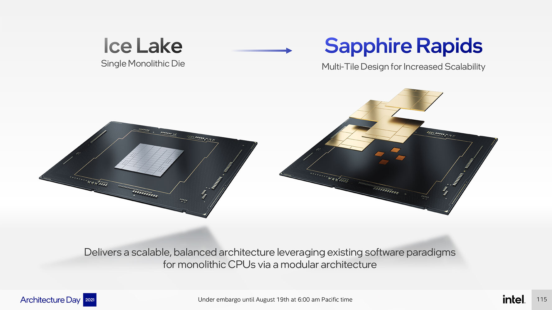
Intel's upcoming Xeon "Sapphire Rapids" processor features a memory interface topology that closely resembles that of first-generation AMD EPYC "Rome," thanks to the multi-chip module design of the processor. Back in 2017, Intel's competing "Skylake-SP" Xeon processors were based on monolithic dies. Despite being spread across multiple memory controller tiles, the 6-channel DDR4 memory interface was depicted by Intel as an advantage over EPYC "Rome." AMD's first "Zen" based enterprise processor was a multi-chip module of four 14 nm, 8-core "Zeppelin" dies, each with a 2-channel DDR4 memory interface that added up to the processor's 8-channel I/O. Much like "Sapphire Rapids," a CPU core from any of the four dies had access to memory and I/O controlled by any other die, as the four were networked over the Infinity Fabric interconnect in a configuration that essentially resembled "4P on a stick."
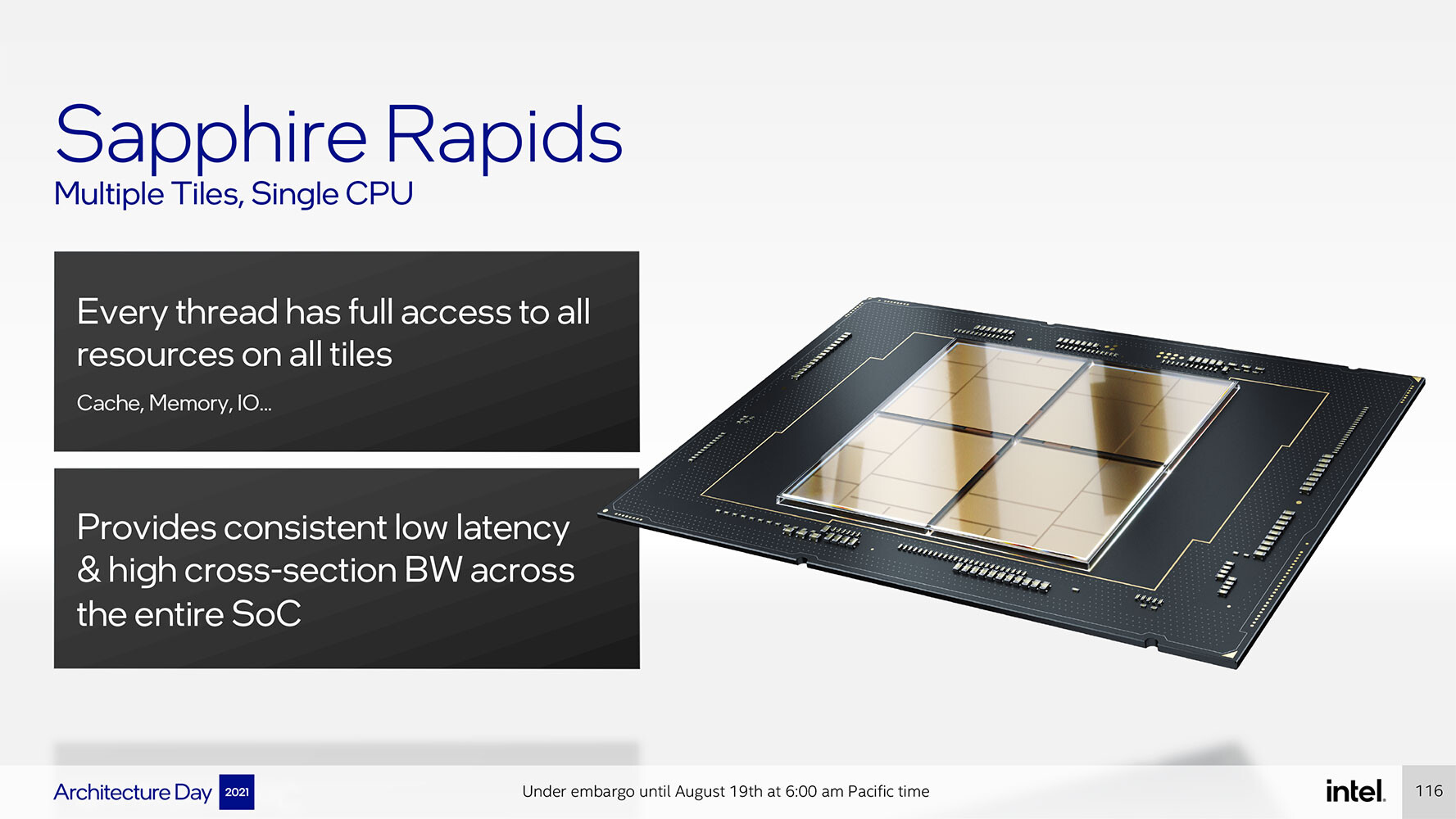
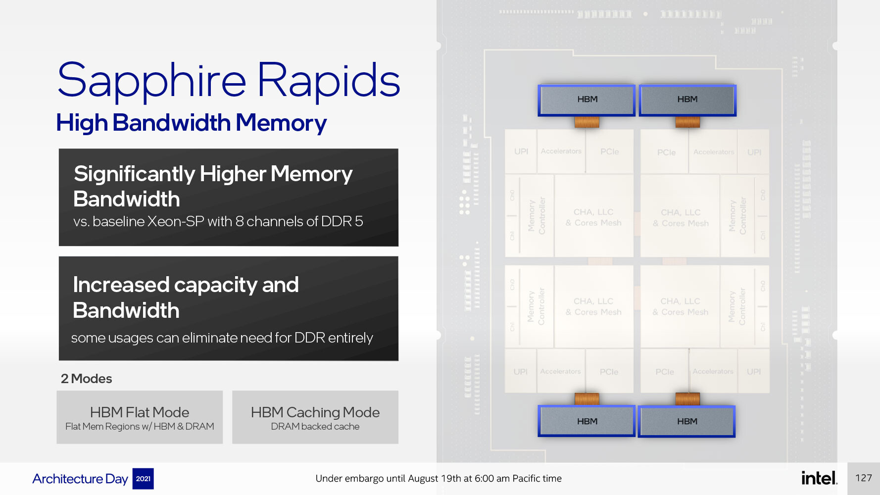
With "Sapphire Rapids," Intel is taking a largely similar approach—it has four compute tiles (dies) instead of a monolithic die, which Intel says helps with scalability in both directions; and each of the four compute tiles has a 2-channel DDR5 or 1024-bit HBM memory interface, which add up to the processor's 8-channel DDR5 total I/O. Intel says that CPU cores from each tile has equal access to memory, last-level cache, and I/O controlled by another die. Inter-tile communication is handled by EMIB physical media (55 micron bump-pitch wiring). UPI 2.0 makes up the inter-socket interconnect. Each of the four compute tiles has 24 UPI 2.0 links that operate at 16 GT/s. Intel didn't detail how memory is presented to the operating system, or the NUMA hierarchy, however much of Intel's engineering effort appears to be focused on making this disjointed memory I/O work as if "Sapphire Rapids" were a monolithic die. The company claims "consistent low-latency, high cross-sectional bandwidth across the SoC."


 Another interesting aspect of "Sapphire Rapids" Xeon processors is support for HBM, which could prove a game-changer for the processor in the HPC and high-density compute markets. Specific models of Xeon "Sapphire Rapids" processors could come with on-package HBM. This memory can either be used as a victim-cache for the on-die caches on the compute tiles, vastly improving the memory sub-system; work exclusively as a standalone main memory; or even work as a non-tiered main memory alongside the DDR5 DRAM with flat memory regions. Intel refers to these as software-visible HBM+DDR5, and software-transparent HBM+DDR5 modes.
With "Sapphire Rapids," Intel is taking a largely similar approach—it has four compute tiles (dies) instead of a monolithic die, which Intel says helps with scalability in both directions; and each of the four compute tiles has a 2-channel DDR5 or 1024-bit HBM memory interface, which add up to the processor's 8-channel DDR5 total I/O. Intel says that CPU cores from each tile has equal access to memory, last-level cache, and I/O controlled by another die. Inter-tile communication is handled by EMIB physical media (55 micron bump-pitch wiring). UPI 2.0 makes up the inter-socket interconnect. Each of the four compute tiles has 24 UPI 2.0 links that operate at 16 GT/s. Intel didn't detail how memory is presented to the operating system, or the NUMA hierarchy, however much of Intel's engineering effort appears to be focused on making this disjointed memory I/O work as if "Sapphire Rapids" were a monolithic die. The company claims "consistent low-latency, high cross-sectional bandwidth across the SoC."


16 Comments on Intel Xeon "Sapphire Rapids" Memory Detailed, Resembles AMD 1st Gen EPYC: Decentralized 8-Channel DDR5
I love the "Up to >100MB shared LLC" bit... so up to (upper bound) greater than (lower bound) 100MB. It's clear it's marketeers and not engineers that wrote this.
I'd expect that there is actually only one tile layout, and Intel didn't actually create two mirrored tile layouts.
That being said: EMIB looks more advanced than what AMD did with Zen1 (and indeed, looks more advanced than even today's Zen3. IIRC, the packaging around the I/O die on Zen3 is a simpler passive connection, and nothing like the microbumps on EMIB). So maybe Intel has a "secret weapon" in there.
videocardz.com/newz/intel-royal-core-project-to-improve-x86-architecture-efficency
[URL='https://www.techpowerup.com/235092/intel-says-amd-epyc-processors-glued-together-in-official-slide-deck']Intel Says AMD EPYC Processors "Glued-together" in Official Slide Deck[/URL]