• Welcome to TechPowerUp Forums, Guest! Please check out our forum guidelines for info related to our community.

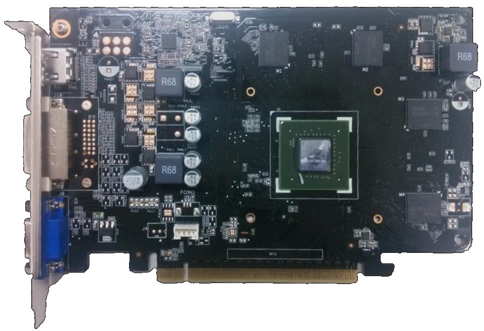
NVIDIA GM107 "Maxwell" Silicon Pictured

Joined
Feb 13, 2012
Messages
522 (0.12/day)
Exactly, they are still on 28Nm and effectively shrank the die by clipping the memory bus, and other changes. But still being 960 Cuda part I can't see some 50% improvement on efficiency, all while higher clocks… on 20Nm perhaps. If they can find a 20% improvement for a 960 Cuda part they'll be doing great. While the 768 Cuda part on GK106 was 110W, I’ve no issue saying they can get it to be 75W.

If wrong and they're better... all the better, but given the information we have to scrutinize it seems to be shaping up as such. Holding to 28Nm is probably one of the biggest limiting issues to the efficiency. Maxwell it's self is evolutionary; it's 20Nm/Denver/UVM that will make it revolutionary.

Well remember this is Maxwell and not Kepler, and nvidia stated Maxwell is designed specifically for mobile and efficiency. If you look at the big picture nvidia started with Fermi all about compute but then back pedaled with Kepler and went all about efficiency and mobile. So each compute unit now has less compute resources and is geared more towards graphics unlike amd where in sea islands they pretty much only improved compute and did almost nothing to the graphics other than some Fine tuning for efficiency. So what do we have now? Bonaire and this gk107 both measuring around 160mm2 but with nvidia packing more cores on the same process. And with nvidia being about 20% faster than gcn per core for graphics intensive tasks, but then being Much behind in compute. It's obvious this is a direct competitor to Bonaire and performing about the same as GTX650boost but closer to a GTX660 when bandwidth is not as needed all with a smaller die meaning better efficiency. And to those who wonder why nvidia would release such a part that performs similar to the ones before? Because nvidia was competing with amds 160mm2 Bonaire with a 220mm2 go106 chip that had a few parts disabled which I bet still cost more.
 
Joined
Apr 30, 2012
Messages
3,881 (0.89/day)
Well remember this is Maxwell and not Kepler, and nvidia stated Maxwell is designed specifically for mobile and efficiency. If you look at the big picture nvidia started with Fermi all about compute but then back pedaled with Kepler and went all about efficiency and mobile. So each compute unit now has less compute resources and is geared more towards graphics unlike amd where in sea islands they pretty much only improved compute and did almost nothing to the graphics other than some Fine tuning for efficiency. So what do we have now? Bonaire and this gk107 both measuring around 160mm2 but with nvidia packing more cores on the same process. And with nvidia being about 20% faster than gcn per core for graphics intensive tasks, but then being Much behind in compute. It's obvious this is a direct competitor to Bonaire and performing about the same as GTX650boost but closer to a GTX660 when bandwidth is not as needed all with a smaller die meaning better efficiency. And to those who wonder why nvidia would release such a part that performs similar to the ones before? Because nvidia was competing with amds 160mm2 Bonaire with a 220mm2 go106 chip that had a few parts disabled which I bet still cost more.

You have to remember and take into account that the results are all on OC 750 Ti models and still not close to a 650 Ti Boost.

650 TI Boost = 768 / 64 / 24
750 Ti = 960 / 80 / 16
R7 260X = 896 / 56 / 16

R7 260X @ $119
R7 260X OC @ $139
GTX 750 @ $119
GTX 750 Ti @ $139-$149

It might be a competitor to the R7 260X after 5months of its release.
 
Last edited:
Joined
Sep 7, 2011
Messages
2,785 (0.60/day)
Location
New Zealand
System Name MoneySink
Processor 2600K @ 4.8
Motherboard P8Z77-V
Cooling AC NexXxos XT45 360, RayStorm, D5T+XSPC tank, Tygon R-3603, Bitspower
Memory 16GB Crucial Ballistix DDR3-1600C8
Video Card(s) GTX 780 SLI (EVGA SC ACX + Giga GHz Ed.)
Storage Kingston HyperX SSD (128) OS, WD RE4 (1TB), RE2 (1TB), Cav. Black (2 x 500GB), Red (4TB)
Display(s) Achieva Shimian QH270-IPSMS (2560x1440) S-IPS
Case NZXT Switch 810
Audio Device(s) onboard Realtek yawn edition
Power Supply Seasonic X-1050
Software Win8.1 Pro
Benchmark Scores 3.5 litres of Pale Ale in 18 minutes.
Well remember this is Maxwell and not Kepler, and nvidia stated Maxwell is designed specifically for mobile and efficiency. If you look at the big picture nvidia started with Fermi all about compute but then back pedaled with Kepler and went all about efficiency and mobile.
I wouldn't confuse an architecture with just the desktop variants of their implementation
So each compute unit now has less compute resources and is geared more towards graphics unlike amd where in sea islands they pretty much only improved compute and did almost nothing to the graphics other than some Fine tuning for efficiency.
Likewise, Nvidia have prioritized floating point calc over integer since the G80, since the pro markets are geared more towards FP optimization. It also the reason that AMD's architectures excel at hashing (primarily an integer function that benefits greatly from AMD's integer shift implementation, and likely the compute unit-to-core ratio AMD has instituted- something that won't change if GM107 moves from 192 to 256 cores per SMX. Compute functionality covers a multitude of variables, and depending on workload and coding optimization can yield a varied array of "wins" and "losses" - further complicated by the fact that Nvidia deliberately cripples features in desktop SKUs to protect a lucrative pro market.
 
Joined
Apr 19, 2011
Messages
2,198 (0.46/day)
Location
So. Cal.
Well remember this is Maxwell and not Kepler, and nvidia stated Maxwell is designed specifically for mobile and efficiency. .
But are we hearing that there's a big change in the basic Cuda functions?

Because nvidia was competing with amds 160mm2 Bonaire with a 220mm2 go106 chip that had a few parts disabled which I bet still cost more.
I believe you mean wasn't... I think the 192-Bit bus was overkill and draws to much for what it brought in performance. Getting off 192-Bit saves on the die while improvement the 128-Bit provides plenty of useable Bandwidth while more efficient.
 
Joined
Sep 7, 2011
Messages
2,785 (0.60/day)
Location
New Zealand
System Name MoneySink
Processor 2600K @ 4.8
Motherboard P8Z77-V
Cooling AC NexXxos XT45 360, RayStorm, D5T+XSPC tank, Tygon R-3603, Bitspower
Memory 16GB Crucial Ballistix DDR3-1600C8
Video Card(s) GTX 780 SLI (EVGA SC ACX + Giga GHz Ed.)
Storage Kingston HyperX SSD (128) OS, WD RE4 (1TB), RE2 (1TB), Cav. Black (2 x 500GB), Red (4TB)
Display(s) Achieva Shimian QH270-IPSMS (2560x1440) S-IPS
Case NZXT Switch 810
Audio Device(s) onboard Realtek yawn edition
Power Supply Seasonic X-1050
Software Win8.1 Pro
Benchmark Scores 3.5 litres of Pale Ale in 18 minutes.
Nvidia could just paper launch a reference card that doesn't need a 6pin and let the partners add a 6pin. Nvidia can say it doesn't need one but the partners added.
That was what I was inferring earlier, although I'd say that the no external power will be the norm in most cases. I'm sure the overclocked versions will gain more publicity, but that is always the case on enthusiast sites, but the bread an butter cards will likely not need external power. I'd also think that a reference cooler might only be for OEM use- I'd expect most AIBs to have their own implementation.
Reference PCB shows option for PCI-E 6-pin, but not used in this case

But still being 960 Cuda part I can't see some 50% improvement on efficiency, all while higher clocks… on 20Nm perhaps. If they can find a 20% improvement for a 960 Cuda part they'll be doing great. While the 768 Cuda part on GK106 was 110W
I thought it had been established that the fully enabled part was a 640 core part, and the non-Ti 750 was to use a 512 core (1 SMX disabled) die
 
Top