• Welcome to TechPowerUp Forums, Guest! Please check out our forum guidelines for info related to our community.

Intel Switches Gears to 7nm Post 10nm, First Node Live in 2021

btarunr

Editor & Senior Moderator
Staff member
Joined
Oct 9, 2007
Messages
46,383 (7.68/day)
Location
Hyderabad, India
System Name RBMK-1000
Processor AMD Ryzen 7 5700G
Motherboard ASUS ROG Strix B450-E Gaming
Cooling DeepCool Gammax L240 V2
Memory 2x 8GB G.Skill Sniper X
Video Card(s) Palit GeForce RTX 2080 SUPER GameRock
Storage Western Digital Black NVMe 512GB
Display(s) BenQ 1440p 60 Hz 27-inch
Case Corsair Carbide 100R
Audio Device(s) ASUS SupremeFX S1220A
Power Supply Cooler Master MWE Gold 650W
Mouse ASUS ROG Strix Impact
Keyboard Gamdias Hermes E2
Software Windows 11 Pro
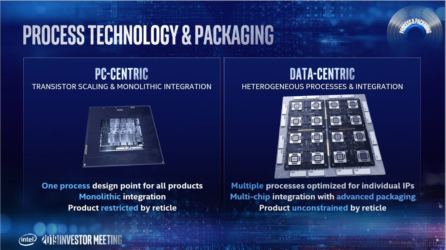
Intel's semiconductor manufacturing business has had a terrible past 5 years as it struggled to execute its 10 nanometer roadmap forcing the company's processor designers to re-hash the "Skylake" microarchitecture for 5 generations of Core processors, including the upcoming "Comet Lake." Its truly next-generation microarchitecture, codenamed "Ice Lake," which features a new CPU core design called "Sunny Cove," comes out toward the end of 2019, with desktop rollouts expected 2020. It turns out that the 10 nm process it's designed for, will have a rather short reign at Intel's fabs. Speaking at an investor's summit on Wednesday, Intel put out its silicon fabrication roadmap that sees an accelerated roll-out of Intel's own 7 nm process.

When it goes live and fit for mass production some time in 2021, Intel's 7 nm process will be a staggering 3 years behind TSMC, which fired up its 7 nm node in 2018. AMD is already mass-producing CPUs and GPUs on this node. Unlike TSMC, Intel will implement EUV (extreme ultraviolet) lithography straightaway. TSMC began 7 nm with DUV (deep ultraviolet) in 2018, and its EUV node went live in March. Samsung's 7 nm EUV node went up last October. Intel's roadmap doesn't show a leap from its current 10 nm node to 7 nm EUV, though. Intel will refine the 10 nm node to squeeze out energy-efficiency, with a refreshed 10 nm+ node that goes live some time in 2020.


The transition from 10 nm+ to 7 nm EUV will significantly increase transistor-densities. Intel is also making the manufacturing process efficient, by reducing "design rules" by 4 times, giving chip-designers more flexibility and creative freedom in the way they design nanoscopic circuitry. The process will also be optimized for heterogeneous chip designs, Foveros packaging (a very advanced form of MCM), and EMIB (reduced footprint interposer).

The 7 nm EUV node will receive two major updates in quick succession. The 7 nm+ node is slated for 2022, and succeeding 7 nm++ node in 2023. Intel did not detail the two besides illustrating performance/Watt gains by almost as much as the transition from 10 nm+ to 7 nm. Elsewhere in the market, the early 2020s could see TSMC 6 nm EUV take center-stage, and Samsung implement its 5 nm EUV node.


Intel will build an Xe enterprise GPGPU based on 7 nm EUV for market release in 2021. The company was specific in mentioning that an "enterprise GP-GPU" will be built on it, and not its entire Xe lineup that includes client-segment, professional, and cloud GPUs. The Xe discrete GPU team, led by Raja Koduri, is probably making a ropewalk, by giving Intel "something" to build on its own fabs, while seeking out Samsung's cutting-edge 5 nm EUV node for the rest of its lineup. Intel confirmed that the its first 7 nm product will be a GPGPU, followed closely by a server CPU.

View at TechPowerUp Main Site
 
Joined
Sep 15, 2007
Messages
3,944 (0.65/day)
Location
Police/Nanny State of America
Processor OCed 5800X3D
Motherboard Asucks C6H
Cooling Air
Memory 32GB
Video Card(s) OCed 6800XT
Storage NVMees
Display(s) 32" Dull curved 1440
Case Freebie glass idk
Audio Device(s) Sennheiser
Power Supply Don't even remember
More lies. This is basically 100% baloney to stop investors from suing, but it's just gonna give them ammo if you ask me. What are they gonna do? Paper launch 6mo ahead for a crappy mobile chip? Release a low core count xeon? It's just sad.
 
Joined
Apr 30, 2012
Messages
3,881 (0.89/day)
They said their 7nm would be the first with EUV? So no EUV for 10nm. Thought that was a big portion for the delay.
 
Joined
Feb 11, 2009
Messages
5,403 (0.97/day)
System Name Cyberline
Processor Intel Core i7 2600k -> 12600k
Motherboard Asus P8P67 LE Rev 3.0 -> Gigabyte Z690 Auros Elite DDR4
Cooling Tuniq Tower 120 -> Custom Watercoolingloop
Memory Corsair (4x2) 8gb 1600mhz -> Crucial (8x2) 16gb 3600mhz
Video Card(s) AMD RX480 -> RX7800XT
Storage Samsung 750 Evo 250gb SSD + WD 1tb x 2 + WD 2tb -> 2tb MVMe SSD
Display(s) Philips 32inch LPF5605H (television) -> Dell S3220DGF
Case antec 600 -> Thermaltake Tenor HTCP case
Audio Device(s) Focusrite 2i4 (USB)
Power Supply Seasonic 620watt 80+ Platinum
Mouse Elecom EX-G
Keyboard Rapoo V700
Software Windows 10 Pro 64bit
I find the claim "relentless innovation continues" quite funny coming from Intel tbh.
 

btarunr

Editor & Senior Moderator
Staff member
Joined
Oct 9, 2007
Messages
46,383 (7.68/day)
Location
Hyderabad, India
System Name RBMK-1000
Processor AMD Ryzen 7 5700G
Motherboard ASUS ROG Strix B450-E Gaming
Cooling DeepCool Gammax L240 V2
Memory 2x 8GB G.Skill Sniper X
Video Card(s) Palit GeForce RTX 2080 SUPER GameRock
Storage Western Digital Black NVMe 512GB
Display(s) BenQ 1440p 60 Hz 27-inch
Case Corsair Carbide 100R
Audio Device(s) ASUS SupremeFX S1220A
Power Supply Cooler Master MWE Gold 650W
Mouse ASUS ROG Strix Impact
Keyboard Gamdias Hermes E2
Software Windows 11 Pro
More lies. This is basically 100% baloney to stop investors from suing, but it's just gonna give them ammo if you ask me. What are they gonna do? Paper launch 6mo ahead for a crappy mobile chip? Release a low core count xeon? It's just sad.
Investors will bail regardless. 2021 is too late for 7 nm EUV. By then TSMC and Samsung will have cornered the 6 nm EUV market with a mature node, and Samsung will begin 5 nm EUV.

Even Raja doesn't trust Intel foundry, so he's designing a token Xe product (a Larrabee-like GPGPU accelerator) for Intel 7 nm EUV, while every other Xe GPU will be built on Samsung 5 nm EUV.
 
Joined
Feb 3, 2017
Messages
3,481 (1.32/day)
Processor R5 5600X
Motherboard ASUS ROG STRIX B550-I GAMING
Cooling Alpenföhn Black Ridge
Memory 2*16GB DDR4-2666 VLP @3800
Video Card(s) EVGA Geforce RTX 3080 XC3
Storage 1TB Samsung 970 Pro, 2TB Intel 660p
Display(s) ASUS PG279Q, Eizo EV2736W
Case Dan Cases A4-SFX
Power Supply Corsair SF600
Mouse Corsair Ironclaw Wireless RGB
Keyboard Corsair K60
VR HMD HTC Vive
2021 is too late for 7 nm EUV. By then TSMC and Samsung will have cornered the 6 nm EUV market with a mature node, and Samsung will begin 5 nm EUV.
The inconsistencies with node naming remain. Intel 7nm is roughly the same as TSMC/Samsung 5nm.
TSMC intends their 5nm to start volume production in the end of 2020.

Edit:
btarunr said:
When it goes live and fit for mass production some time in 2021, Intel's 7 nm process will be a staggering 3 years behind TSMC, which fired up its 7 nm node in 2018. AMD is already mass-producing CPUs and GPUs on this node. Unlike TSMC, Intel will implement EUV (extreme ultraviolet) lithography straightaway. TSMC began 7 nm with DUV (deep ultraviolet) in 2018, and its EUV node went live in March. Samsung's 7 nm EUV node went up last October. Intel's roadmap doesn't show a leap from its current 10 nm node to 7 nm EUV, though. Intel will refine the 10 nm node to squeeze out energy-efficiency, with a refreshed 10 nm+ node that goes live some time in 2020.
So, point by point:
1. Intel 7nm (mass production 2021) is comparable to TSMC 5nm (volume production end of 2020). That is on 4th slide as well.
2. Intel has no choice when it comes to EUV due to feature sizes on a small node. 7nm (and Intel's 10nm) are right on the line where not using EUV is still feasible but barely. Both TSMC and Samsung are starting to partially use EUV on 7nm (7nm+ for TSMC and Samsung right away). EUV has some teething problems, technical side of things has been mostly worked out but tooling availability is still a problem and things just take time.
3. Intel's roadmap is curious, both in terms of foundry and CPUs. Looks like there will be very limited Intel 10nm and despite fast 10nm iterations they intend to largely skip it and shoot for 7nm in 2021. This makes perfect sense both financially as well as technically. Setting up foundries for a node is expensive (billions, with a B) and time consuming. If the intended lifetime of a node is about a year before the next one is ready, it would not make much sense to widely adopt the node.
 
Last edited:
Joined
May 13, 2014
Messages
21 (0.01/day)
System Name Project Taco
Processor i7 4770k
Motherboard Gigabyte G1 Sniper 5 z87
Cooling Corsair H100i w/Noiseblocker eLoop
Memory Avexir Core Series White LED 4x4GB 1600mhz
Video Card(s) 2x EVGA Nvidia GTX 780 TI Classified
Storage Samsung 840 EVO 500GB
Display(s) 2 QNIX QX2710
Case NZXT H440
Audio Device(s) O2/ODAC
Power Supply EVGA Supernova 1000W Gold
Investors will bail regardless. 2021 is too late for 7 nm EUV. By then TSMC and Samsung will have cornered the 6 nm EUV market with a mature node, and Samsung will begin 5 nm EUV.

Even Raja doesn't trust Intel foundry, so he's designing a token Xe product (a Larrabee-like GPGPU accelerator) for Intel 7 nm EUV, while every other Xe GPU will be built on Samsung 5 nm EUV.

What TSMC is offering as "7nm" isn't 7nm at all. The fact that they're using DUV is proof of that. DUV is a fancy word for slightly more advanced current lithography methodologies (using the 193nm excimer laser). NOW that they just got their EUV machines from ASML (which use 13.5nm EUV as a source) a few months back they could be doing proper 7nm, but even then they're only using it for "four non-critical layers" of the wafer process. That in itself is indication that their naming nomenclature doesn't really stack up. Their proper 7nm is likely to be the 7nm+ or 6nm that they've been discussing, where they will use full on EUV for the lithography process.
 
Joined
Feb 3, 2017
Messages
3,481 (1.32/day)
Processor R5 5600X
Motherboard ASUS ROG STRIX B550-I GAMING
Cooling Alpenföhn Black Ridge
Memory 2*16GB DDR4-2666 VLP @3800
Video Card(s) EVGA Geforce RTX 3080 XC3
Storage 1TB Samsung 970 Pro, 2TB Intel 660p
Display(s) ASUS PG279Q, Eizo EV2736W
Case Dan Cases A4-SFX
Power Supply Corsair SF600
Mouse Corsair Ironclaw Wireless RGB
Keyboard Corsair K60
VR HMD HTC Vive
What TSMC is offering as "7nm" isn't 7nm at all. The fact that they're using DUV is proof of that. DUV is a fancy word for slightly more advanced current lithography methodologies (using the 193nm excimer laser). NOW that they just got their EUV machines from ASML (which use 13.5nm EUV as a source) a few months back they could be doing proper 7nm, but even then they're only using it for "four non-critical layers" of the wafer process. That in itself is indication that their naming nomenclature doesn't really stack up. Their proper 7nm is likely to be the 7nm+ or 6nm that they've been discussing, where they will use full on EUV for the lithography process.
Naming nomenclatures do not stack up in general. This went all the way to hell several nodes ago and today the name does not match up to any particular feature size. Different foundries naming the nodes differently is not new either.

TSMC is using EUV on 4 non-critical layers on their 7nm+ node. They have not been very specific but 5nm is going to use - at least mostly, if not completely - EUV. The intermediate 6nm seems to be in large part just from extended use of EUV on otherwise 7nm node. Samsung is following largely the same path except they skipped doing 7nm without any EUV.
 
Joined
May 13, 2014
Messages
21 (0.01/day)
System Name Project Taco
Processor i7 4770k
Motherboard Gigabyte G1 Sniper 5 z87
Cooling Corsair H100i w/Noiseblocker eLoop
Memory Avexir Core Series White LED 4x4GB 1600mhz
Video Card(s) 2x EVGA Nvidia GTX 780 TI Classified
Storage Samsung 840 EVO 500GB
Display(s) 2 QNIX QX2710
Case NZXT H440
Audio Device(s) O2/ODAC
Power Supply EVGA Supernova 1000W Gold
Naming nomenclatures do not stack up in general. This went all the way to hell several nodes ago and today the name does not match up to any particular feature size. Different foundries naming the nodes differently is not new either.

TSMC is using EUV on 4 non-critical layers on their 7nm+ node. They have not been very specific but 5nm is going to use - at least mostly, if not completely - EUV. The intermediate 6nm seems to be in large part just from extended use of EUV on otherwise 7nm node. Samsung is following largely the same path except they skipped doing 7nm without any EUV.
Problem with that is 193nm excimers you aren't able to actually get to ITRS spec for 7nm. You can't have enough refractory lenses set to do it efficiently and immersion lithography isn't enough to get you to that point properly either last i checked. My whole point was that what they're calling 7nm is anything but.
 
Joined
Feb 3, 2017
Messages
3,481 (1.32/day)
Processor R5 5600X
Motherboard ASUS ROG STRIX B550-I GAMING
Cooling Alpenföhn Black Ridge
Memory 2*16GB DDR4-2666 VLP @3800
Video Card(s) EVGA Geforce RTX 3080 XC3
Storage 1TB Samsung 970 Pro, 2TB Intel 660p
Display(s) ASUS PG279Q, Eizo EV2736W
Case Dan Cases A4-SFX
Power Supply Corsair SF600
Mouse Corsair Ironclaw Wireless RGB
Keyboard Corsair K60
VR HMD HTC Vive
Problem with that is 193nm excimers you aren't able to actually get to ITRS spec for 7nm. You can't have enough refractory lenses set to do it efficiently and immersion lithography isn't enough to get you to that point properly either last i checked. My whole point was that what they're calling 7nm is anything but.
SAQP? Definitely cannot be done efficiently but it is kind of possible. I believe the understanding is that EUV becomes necessary when going to under 40nm metal pitch. Of course, this is a vast simplification but seems to be a very good indicator. This, incidentally, is where TSMC stayed at while Samsung and Intel went below (36nm for both if my memory serves right).

By the way, what is ITRS spec for 7nm? Quick Google didn't give me a proper answer, hoping you have a link at hand :)
 
Joined
Sep 15, 2007
Messages
3,944 (0.65/day)
Location
Police/Nanny State of America
Processor OCed 5800X3D
Motherboard Asucks C6H
Cooling Air
Memory 32GB
Video Card(s) OCed 6800XT
Storage NVMees
Display(s) 32" Dull curved 1440
Case Freebie glass idk
Audio Device(s) Sennheiser
Power Supply Don't even remember
What TSMC is offering as "7nm" isn't 7nm at all. The fact that they're using DUV is proof of that. DUV is a fancy word for slightly more advanced current lithography methodologies (using the 193nm excimer laser). NOW that they just got their EUV machines from ASML (which use 13.5nm EUV as a source) a few months back they could be doing proper 7nm, but even then they're only using it for "four non-critical layers" of the wafer process. That in itself is indication that their naming nomenclature doesn't really stack up. Their proper 7nm is likely to be the 7nm+ or 6nm that they've been discussing, where they will use full on EUV for the lithography process.

But it doesn't matter when it's actually profitable with high yields...unlike the 500 lb baby monkey flailing around.
 
Joined
Feb 25, 2016
Messages
382 (0.13/day)
System Name 06/2023
Processor R7 7800X3D
Motherboard ROG STRIX B650E-I GAMING WIFI
Cooling Custom 240mm cooling (for CPU) with noctua nfa12x25 and Phantek T30
Memory 32gb Gskill 6000 CL30
Video Card(s) RTX 4070 dual asus deshrouded with 120mm NF-A12x25
Storage 2tb samsung 990 pro + 4tb samsung 870 evo
Display(s) Asus 27" Oled PG27AQDM + Asus 27" IPS PG279QM
Case Ncase M1 v6.1
Audio Device(s) Steelseries arctis pro wireless + Shure SM7b with Steinberg UR
Power Supply Corsair SF750 Platinum
Mouse Corsair scimitar pro (this mouse need an overall guys pls) + Logitech G Pro wireless with powerplay
Keyboard Sharkoon purewriter
Software windows 11
Benchmark Scores Over 9000 !
Investors will bail regardless. 2021 is too late for 7 nm EUV. By then TSMC and Samsung will have cornered the 6 nm EUV market with a mature node, and Samsung will begin 5 nm EUV.

Even Raja doesn't trust Intel foundry, so he's designing a token Xe product (a Larrabee-like GPGPU accelerator) for Intel 7 nm EUV, while every other Xe GPU will be built on Samsung 5 nm EUV.

Wtf ? you don't know that Intel process have always been smaller than other manufacturers??? I am really disappointed to see this kinda of comment on Techpowerup!
 
Joined
Feb 18, 2005
Messages
5,238 (0.75/day)
Location
Ikenai borderline!
System Name Firelance.
Processor Threadripper 3960X
Motherboard ROG Strix TRX40-E Gaming
Cooling IceGem 360 + 6x Arctic Cooling P12
Memory 8x 16GB Patriot Viper DDR4-3200 CL16
Video Card(s) MSI GeForce RTX 4060 Ti Ventus 2X OC
Storage 2TB WD SN850X (boot), 4TB Crucial P3 (data)
Display(s) 3x AOC Q32E2N (32" 2560x1440 75Hz)
Case Enthoo Pro II Server Edition (Closed Panel) + 6 fans
Power Supply Fractal Design Ion+ 2 Platinum 760W
Mouse Logitech G602
Keyboard Logitech G613
Software Windows 10 Professional x64
Seems like 7nm is finally the ticket to Intel getting back on track. They're only dedicating resources to 10nm because they have designs for it that they don't have time to redo for 7nm.

Reading more and more about their 10nm fiasco, it seems a lot of the issue was that Intel needed EUV to make it actually work, but the technology literally wasn't available. So they were forced to attempt to implement the far-more-complex multi-patterning... which has finally come right, just in time for EUV to be practical. Well, that's the risk of being a tech leader; sometimes you are forced to take detours, and sometimes those detours end up being dead ends.
 
Joined
Sep 15, 2007
Messages
3,944 (0.65/day)
Location
Police/Nanny State of America
Processor OCed 5800X3D
Motherboard Asucks C6H
Cooling Air
Memory 32GB
Video Card(s) OCed 6800XT
Storage NVMees
Display(s) 32" Dull curved 1440
Case Freebie glass idk
Audio Device(s) Sennheiser
Power Supply Don't even remember
What makes it crappy?

Don't think this qualifies as a paper launch.

Zero details, just vauge references.... Hint: It's worse than the current ones and apparently nowhere near actually making it into products.
 
Joined
May 31, 2017
Messages
877 (0.35/day)
Location
Home
System Name Blackbox
Processor AMD Ryzen 7 3700X
Motherboard Asus TUF B550-Plus WiFi
Cooling Scythe Fuma 2
Memory 2x8GB DDR4 G.Skill FlareX 3200Mhz CL16
Video Card(s) MSI RTX 3060 Ti Gaming Z
Storage Kingston KC3000 1TB + WD SN550 1TB + Samsung 860 QVO 1TB
Display(s) LG 27GP850-B
Case Lian Li O11 Air Mini
Audio Device(s) Logitech Z200
Power Supply Seasonic Focus+ Gold 750W
Mouse Logitech G305
Keyboard MasterKeys Pro S White (MX Brown)
Software Windows 10
Benchmark Scores It plays games.
Yeah.. I'll believe it when I see it.
 
Joined
Oct 28, 2010
Messages
251 (0.05/day)
What intel 10nm ?

For now, intel states that "is nearly ready to ship 10-nanometer processors in large volumes "... in June.
 
Joined
Sep 15, 2007
Messages
3,944 (0.65/day)
Location
Police/Nanny State of America
Processor OCed 5800X3D
Motherboard Asucks C6H
Cooling Air
Memory 32GB
Video Card(s) OCed 6800XT
Storage NVMees
Display(s) 32" Dull curved 1440
Case Freebie glass idk
Audio Device(s) Sennheiser
Power Supply Don't even remember
What intel 10nm ?

For now, intel states that "is nearly ready to ship 10-nanometer processors in large volumes "... in June.

So ready they only have "simulated" performance numbers for em. Intel should write a book, "How to become the laughing stock of the tech industry in these 10 easy steps!"
 

SL2

Joined
Jan 27, 2006
Messages
1,807 (0.27/day)
Intel had a test system running last year, possibly running at 1 GHz for all we know, but my point is that it's not all slides at this point.


If you WANT it to be crappy, that's a whole different thing, but it's not much to make an assumption out of. :D If anything, I'm a AMD fan myself, and I'd like to see AMD take some of the CPU market share, but this isn't a paper launch. You need model numbers, price, launch dates, performance tests and maybe even reviews for that.

It may still be crap, but we have zero evidence that it is. The fact that Intel stayed at 4 core and 14 nm forever, or changes the socket too often, or sells multiplier locked CPU's, or calls the 9900K a 95 W SKU isn't evidence for Ice Lake being crap.
 
Last edited:
Joined
Jun 10, 2014
Messages
2,902 (0.80/day)
Processor AMD Ryzen 9 5900X ||| Intel Core i7-3930K
Motherboard ASUS ProArt B550-CREATOR ||| Asus P9X79 WS
Cooling Noctua NH-U14S ||| Be Quiet Pure Rock
Memory Crucial 2 x 16 GB 3200 MHz ||| Corsair 8 x 8 GB 1333 MHz
Video Card(s) MSI GTX 1060 3GB ||| MSI GTX 680 4GB
Storage Samsung 970 PRO 512 GB + 1 TB ||| Intel 545s 512 GB + 256 GB
Display(s) Asus ROG Swift PG278QR 27" ||| Eizo EV2416W 24"
Case Fractal Design Define 7 XL x 2
Audio Device(s) Cambridge Audio DacMagic Plus
Power Supply Seasonic Focus PX-850 x 2
Mouse Razer Abyssus
Keyboard CM Storm QuickFire XT
Software Ubuntu
Intel's 7 nm process will be a staggering 3 years behind TSMC, which fired up its 7 nm node in 2018. AMD is already mass-producing CPUs and GPUs on this node.
You should know better than to compare TSMC 7nm with Intel 7nm when it's actually comparable to Intel's 10nm.

For the record;
Intel was first to ship a product on this generation of nodes in April 2018 followed by AMD in ~December 2018, but neither have shipped volumes yet. But at least AMD have shipped the largest chip so far, and both expect to ship "volumes" in Q3 2019.
 
Joined
Feb 18, 2005
Messages
5,238 (0.75/day)
Location
Ikenai borderline!
System Name Firelance.
Processor Threadripper 3960X
Motherboard ROG Strix TRX40-E Gaming
Cooling IceGem 360 + 6x Arctic Cooling P12
Memory 8x 16GB Patriot Viper DDR4-3200 CL16
Video Card(s) MSI GeForce RTX 4060 Ti Ventus 2X OC
Storage 2TB WD SN850X (boot), 4TB Crucial P3 (data)
Display(s) 3x AOC Q32E2N (32" 2560x1440 75Hz)
Case Enthoo Pro II Server Edition (Closed Panel) + 6 fans
Power Supply Fractal Design Ion+ 2 Platinum 760W
Mouse Logitech G602
Keyboard Logitech G613
Software Windows 10 Professional x64
You should know better than to compare TSMC 7nm with Intel 7nm when it's actually comparable to Intel's 10nm.

Oh come now, are you really expecting bta to write a 2019 "article" that isn't sensationalist clickbait?
 
Joined
Apr 30, 2011
Messages
2,652 (0.56/day)
Location
Greece
Processor AMD Ryzen 5 5600@80W
Motherboard MSI B550 Tomahawk
Cooling ZALMAN CNPS9X OPTIMA
Memory 2*8GB PATRIOT PVS416G400C9K@3733MT_C16
Video Card(s) Sapphire Radeon RX 6750 XT Pulse 12GB
Storage Sandisk SSD 128GB, Kingston A2000 NVMe 1TB, Samsung F1 1TB, WD Black 10TB
Display(s) AOC 27G2U/BK IPS 144Hz
Case SHARKOON M25-W 7.1 BLACK
Audio Device(s) Realtek 7.1 onboard
Power Supply Seasonic Core GC 500W
Mouse Sharkoon SHARK Force Black
Keyboard Trust GXT280
Software Win 7 Ultimate 64bit/Win 10 pro 64bit/Manjaro Linux
Totally expected move from any rational person following the tech industry and news. Point is, it isn't too certain they will succeed in 7nm either but the possibilities are better for sure. And the main question now is, how far behind Zen arch will the get until they present both a new arch and a feasible and efficient process to battle the one that other fab owners will have then. Imho, the fall of the giant has already begun. Let's hope that competition will exist in a year or so in the consumer CPU market.
 
Joined
Jan 13, 2018
Messages
157 (0.07/day)
System Name N/A
Processor Intel Core i5 3570
Motherboard Gigabyte B75
Cooling Coolermaster Hyper TX3
Memory 12 GB DDR3 1600
Video Card(s) MSI Gaming Z RTX 2060
Storage SSD
Display(s) Samsung 4K HDR 60 Hz TV
Case Eagle Warrior Gaming
Audio Device(s) N/A
Power Supply Coolermaster Elite 460W
Mouse Vorago KM500
Keyboard Vorago KM500
Software Windows 10
Benchmark Scores N/A
They're only dedicating resources to 10nm because they have designs for it that they don't have time to redo for 7nm.

Reading more and more about their 10nm fiasco, it seems a lot of the issue was that Intel needed EUV to make it actually work, but the technology literally wasn't available. So they were forced to attempt to implement the far-more-complex multi-patterning...

I totally agree, Intel's 10 nm is too dense for DUV, that is why it will never be a good process, Intel was too ambitious. TSMC's 7 nm worked out in DUV cause is less denser than Intel's 10 nm. By comparison an Apple A12 has around 82.86 MTr/mm2 and Intel Cannon Lake around 90.78 MTr/mm2.

I think that desktops will never see a 10 nm product, cause Comet Lake will launch in Q1 2020 and Rocket Lake in Q1 2021 both using 14 nm, Golden Cove would launch at the end of 2021 in 7 nm for desktop. So desktops will skip both Ice Lake and Tiger Lake in 10 nm (and Cannon Lake which by now is more than certain that is dropped).

By the way, what is ITRS spec for 7nm? Quick Google didn't give me a proper answer, hoping you have a link at hand :)

https://irds.ieee.org/images/files/pdf/2017/2017IRDS_MM.pdf page 12
 
Joined
Apr 12, 2013
Messages
6,750 (1.67/day)
They may or they may not, I doubt even Intel knows what they'll release next :shadedshu:


Top