- Joined
- Oct 9, 2007
- Messages
- 47,895 (7.37/day)
- Location
- Dublin, Ireland
| System Name | RBMK-1000 |
|---|---|
| Processor | AMD Ryzen 7 5700G |
| Motherboard | Gigabyte B550 AORUS Elite V2 |
| Cooling | DeepCool Gammax L240 V2 |
| Memory | 2x 16GB DDR4-3200 |
| Video Card(s) | Galax RTX 4070 Ti EX |
| Storage | Samsung 990 1TB |
| Display(s) | BenQ 1440p 60 Hz 27-inch |
| Case | Corsair Carbide 100R |
| Audio Device(s) | ASUS SupremeFX S1220A |
| Power Supply | Cooler Master MWE Gold 650W |
| Mouse | ASUS ROG Strix Impact |
| Keyboard | Gamdias Hermes E2 |
| Software | Windows 11 Pro |
Samsung Electronics Co., Ltd., a world leader in advanced semiconductor technology, today announced its ongoing commitment to foundry innovation and service at the Samsung Foundry Forum 2019 USA, providing the silicon community with wide-ranging updates on technology advances that support the most demanding applications of today and tomorrow.
The event, held today in Santa Clara, California, features top Samsung executives and industry experts reviewing progress on semiconductor technologies and foundry platform solutions that enable developments in artificial intelligence (AI), machine learning, 5G networking, automotive, the Internet of Things (IoT), advanced data centers and many other domains.
"We stand at the verge of the Fourth Industrial Revolution, a new era of high-performance computing and connectivity that will advance the daily lives of everyone on the planet," said Dr. ES Jung, President and head of Foundry Business at Samsung Electronics.
"Samsung Electronics fully understands that achieving powerful and reliable silicon solutions requires not only the most advanced manufacturing and packaging processes as well as design solutions, but also collaborative foundry-customer relationships grounded on trust and shared vision. This year's Foundry Forum is filled with compelling evidence of our commitment to progress in all those areas, and we're honored to host and converse with our industry's best and brightest," Dr. Jung added.
The new 3nm GAE PDK version 0.1 is ready
Samsung's 3nm Gate-All-Around (GAA) process, 3GAE, development is on track. The company noted today that its Process Design Kit (PDK) version 0.1 for 3GAE has been released in April to help customers get an early start on the design work and enable improved design competitiveness along with reduced turnaround time (TAT).
Compared to 7nm technology, Samsung's 3GAE process is designed to provide up to a 45 percent reduction in chip area with 50 percent lower power consumption or 35 percent higher performance. The GAA-based process node is expected to be widely adopted in next-generation applications, such as mobile, network, automotive, Artificial Intelligence (AI) and IoT.
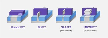
Conventional GAA based on nanowire requires a larger number of stacks due to its small effective channel width. On the other hand, Samsung's patented version of GAA, MBCFET (Multi-Bridge-Channel FET), uses a nanosheet architecture, enabling greater current per stack.
While FinFET structures must modulate the number of fins in a discrete way, MBCFET provides greater design flexibility by controlling the nanosheet width. In addition, MBCFET 's compatibility with FinFET processes means the two can share the same manufacturing technology and equipment, which accelerates process development and production ramp-up.
Samsung recently taped out the 3GAE test vehicle design and will focus on improving its performance and power efficiency going forward.
The launching of a new SAFE-Cloud program
As part of its ongoing efforts to support and enhance customers' entire design workflow, Samsung Electronics launched the Samsung Advanced Foundry Ecosystem Cloud (SAFE -Cloud) program. It will provide customers with a more flexible design environment through collaboration with major public cloud service providers, such as Amazon Web Services (AWS) and Microsoft Azure, as well as leading Electronic Design Automation (EDA) companies, including Cadence and Synopsys.
To date, most foundry customers have built and managed design infrastructure on their own servers. The SAFE-Cloud program reduces this burden and supports easier, faster and more efficient design efforts by providing an excellent turnkey design environment with extensive process information (PDK, design methodologies), EDA tools, design assets (IP, library) and design services.
Customers can be assured of as much server and storage space as they need, as well as a safe environment optimized for chip design, due to Samsung Electronics' verification of SAFE -Cloud's security, applicability and expandability.
Utilizing the SAFE -Cloud platform, Samsung was able to accelerate the development of its 7nm and 5nm cell libraries in collaboration with Synopsys. In addition, Samsung, Gaonchips - a fabless design company in Korea - and Cadence have successfully completed design verification based on the platform.
"Making up-front investments in high-performance computing (HPC) servers and systems can be a challenge for a company like us," said Kyu Dong Jung, CEO of Gaonchips. "SAFETM-Cloud offers us a very flexible design environment without requiring investment in additional infrastructure, as well as reduced design TAT. I expect this program to provide more tangible business and technical benefits to us and the entire fabless industry."
Process technology roadmap and advanced packaging updates
Samsung's roadmap includes four FinFET-based processes from 7nm down to 4nm that leverage extreme ultraviolet (EUV) technology as well as 3nm GAA, or MBCFET .
In the second half of this year, Samsung is scheduled to start the mass production of 6nm process devices and complete the development of 4nm process.
The product design of Samsung's 5nm FinFET process, which was developed in April, is expected to be completed in the second half of this year and go under mass production in the first half of 2020.
Extensions of the company's FD-SOI (FDS) process and eMRAM together with an expanded set of state-of-the-art package solutions were also unveiled at this year's Foundry Forum. Development of the successor to the 28FDS process, 18FDS, and eMRAM with 1Gb capacity will be finished this year.
View at TechPowerUp Main Site
The event, held today in Santa Clara, California, features top Samsung executives and industry experts reviewing progress on semiconductor technologies and foundry platform solutions that enable developments in artificial intelligence (AI), machine learning, 5G networking, automotive, the Internet of Things (IoT), advanced data centers and many other domains.

"We stand at the verge of the Fourth Industrial Revolution, a new era of high-performance computing and connectivity that will advance the daily lives of everyone on the planet," said Dr. ES Jung, President and head of Foundry Business at Samsung Electronics.
"Samsung Electronics fully understands that achieving powerful and reliable silicon solutions requires not only the most advanced manufacturing and packaging processes as well as design solutions, but also collaborative foundry-customer relationships grounded on trust and shared vision. This year's Foundry Forum is filled with compelling evidence of our commitment to progress in all those areas, and we're honored to host and converse with our industry's best and brightest," Dr. Jung added.
The new 3nm GAE PDK version 0.1 is ready
Samsung's 3nm Gate-All-Around (GAA) process, 3GAE, development is on track. The company noted today that its Process Design Kit (PDK) version 0.1 for 3GAE has been released in April to help customers get an early start on the design work and enable improved design competitiveness along with reduced turnaround time (TAT).
Compared to 7nm technology, Samsung's 3GAE process is designed to provide up to a 45 percent reduction in chip area with 50 percent lower power consumption or 35 percent higher performance. The GAA-based process node is expected to be widely adopted in next-generation applications, such as mobile, network, automotive, Artificial Intelligence (AI) and IoT.
Conventional GAA based on nanowire requires a larger number of stacks due to its small effective channel width. On the other hand, Samsung's patented version of GAA, MBCFET (Multi-Bridge-Channel FET), uses a nanosheet architecture, enabling greater current per stack.
While FinFET structures must modulate the number of fins in a discrete way, MBCFET provides greater design flexibility by controlling the nanosheet width. In addition, MBCFET 's compatibility with FinFET processes means the two can share the same manufacturing technology and equipment, which accelerates process development and production ramp-up.
Samsung recently taped out the 3GAE test vehicle design and will focus on improving its performance and power efficiency going forward.
The launching of a new SAFE-Cloud program
As part of its ongoing efforts to support and enhance customers' entire design workflow, Samsung Electronics launched the Samsung Advanced Foundry Ecosystem Cloud (SAFE -Cloud) program. It will provide customers with a more flexible design environment through collaboration with major public cloud service providers, such as Amazon Web Services (AWS) and Microsoft Azure, as well as leading Electronic Design Automation (EDA) companies, including Cadence and Synopsys.
To date, most foundry customers have built and managed design infrastructure on their own servers. The SAFE-Cloud program reduces this burden and supports easier, faster and more efficient design efforts by providing an excellent turnkey design environment with extensive process information (PDK, design methodologies), EDA tools, design assets (IP, library) and design services.
Customers can be assured of as much server and storage space as they need, as well as a safe environment optimized for chip design, due to Samsung Electronics' verification of SAFE -Cloud's security, applicability and expandability.
Utilizing the SAFE -Cloud platform, Samsung was able to accelerate the development of its 7nm and 5nm cell libraries in collaboration with Synopsys. In addition, Samsung, Gaonchips - a fabless design company in Korea - and Cadence have successfully completed design verification based on the platform.
"Making up-front investments in high-performance computing (HPC) servers and systems can be a challenge for a company like us," said Kyu Dong Jung, CEO of Gaonchips. "SAFETM-Cloud offers us a very flexible design environment without requiring investment in additional infrastructure, as well as reduced design TAT. I expect this program to provide more tangible business and technical benefits to us and the entire fabless industry."
Process technology roadmap and advanced packaging updates
Samsung's roadmap includes four FinFET-based processes from 7nm down to 4nm that leverage extreme ultraviolet (EUV) technology as well as 3nm GAA, or MBCFET .
In the second half of this year, Samsung is scheduled to start the mass production of 6nm process devices and complete the development of 4nm process.
The product design of Samsung's 5nm FinFET process, which was developed in April, is expected to be completed in the second half of this year and go under mass production in the first half of 2020.
Extensions of the company's FD-SOI (FDS) process and eMRAM together with an expanded set of state-of-the-art package solutions were also unveiled at this year's Foundry Forum. Development of the successor to the 28FDS process, 18FDS, and eMRAM with 1Gb capacity will be finished this year.
View at TechPowerUp Main Site


")