- Joined
- Oct 9, 2007
- Messages
- 46,371 (7.67/day)
- Location
- Hyderabad, India
| System Name | RBMK-1000 |
|---|---|
| Processor | AMD Ryzen 7 5700G |
| Motherboard | ASUS ROG Strix B450-E Gaming |
| Cooling | DeepCool Gammax L240 V2 |
| Memory | 2x 8GB G.Skill Sniper X |
| Video Card(s) | Palit GeForce RTX 2080 SUPER GameRock |
| Storage | Western Digital Black NVMe 512GB |
| Display(s) | BenQ 1440p 60 Hz 27-inch |
| Case | Corsair Carbide 100R |
| Audio Device(s) | ASUS SupremeFX S1220A |
| Power Supply | Cooler Master MWE Gold 650W |
| Mouse | ASUS ROG Strix Impact |
| Keyboard | Gamdias Hermes E2 |
| Software | Windows 11 Pro |
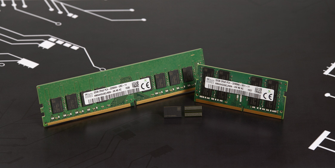
SK hynix Inc. announced today that it has developed 1Znm 16Gb (Gigabits) DDR4 (Double Data Rate 4) DRAM. As 16Gb is the industry's largest density for a single chip, the total memory capacity per wafer is also the largest of the existing DRAMs. The productivity of this product has improved by about 27% compared to the previous generation, 1Y nm. It does not require highly expensive extreme ultraviolet (EUV) lithography, which gives it a competitive edge cost-wise.
The new 1Z nm DRAM also supports a data transfer rate of up to 3,200 Mbps, which is the fastest data processing speed in DDR4 interface. The Company significantly increased its power efficiency, successfully reducing power consumption by about 40% compared to modules of the same density made with 1Y nm 8 Gb DRAM.

In particular, SK hynix applied a new substance not used in the manufacturing process of the previous generation, maximizing the capacitance of this 1Znm product. Capacitance, the amount of electrical charge a capacitor can store, is a key element of DRAM operation. A new design has also been introduced to increase operational stability.
"1Znm DDR4 DRAM boasts the industry's highest density, speed, and power efficiency, making it the best product to meet the changing demands of customers seeking high-performance/high-density DRAM," said Lee Jung-hoon, Head of 1Z TF of DRAM Development & Business. "SK hynix will start mass production and full-scale delivery next year to actively respond to market demand."
SK hynix plans to expand the 1Znm technology process to a variety of applications, such as LPDDR5, the next generation mobile DRAM, and HBM3, the fastest DRAM to be.
View at TechPowerUp Main Site
The new 1Z nm DRAM also supports a data transfer rate of up to 3,200 Mbps, which is the fastest data processing speed in DDR4 interface. The Company significantly increased its power efficiency, successfully reducing power consumption by about 40% compared to modules of the same density made with 1Y nm 8 Gb DRAM.
In particular, SK hynix applied a new substance not used in the manufacturing process of the previous generation, maximizing the capacitance of this 1Znm product. Capacitance, the amount of electrical charge a capacitor can store, is a key element of DRAM operation. A new design has also been introduced to increase operational stability.
"1Znm DDR4 DRAM boasts the industry's highest density, speed, and power efficiency, making it the best product to meet the changing demands of customers seeking high-performance/high-density DRAM," said Lee Jung-hoon, Head of 1Z TF of DRAM Development & Business. "SK hynix will start mass production and full-scale delivery next year to actively respond to market demand."
SK hynix plans to expand the 1Znm technology process to a variety of applications, such as LPDDR5, the next generation mobile DRAM, and HBM3, the fastest DRAM to be.
View at TechPowerUp Main Site


