• Welcome to TechPowerUp Forums, Guest! Please check out our forum guidelines for info related to our community.

Samsung Demonstrates 256 Gb 3 nm MBCFET Chip at ISSCC 2021

AleksandarK

News Editor
Staff member
Joined
Aug 19, 2017
Messages
2,232 (0.91/day)
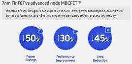
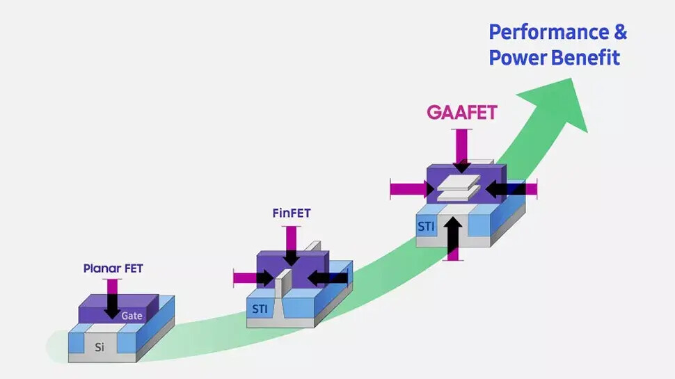
During the IEEE International Solid-State Circuits Conference (ISSCC), Samsung Foundry has presented a new step towards smaller and more efficient nodes. The new chip that was presented is a 256 Gb memory chip, based on SRAM technology. However, all of that doesn't sound interesting, until we mention the technology that is behind it. Samsung has for the first time manufactured a chip using the company's gate-all-around field-effect transistor (GAAFET) technology on the 3 nm semiconductor node. Formally, there are two types of GAAFET technology: the regular GAAFET that uses nanowires as fins of the transistor, and MBCFET (multi-bridge channel FET) that uses thicker fins that come in a form of a nanosheet.

Samsung has demonstrated the first SRAM chip that uses MBCFET technology today. The chip in question is a 256 Gb chip with an area of 56 mm². The achievement Samsung is proud of is that the chip uses 230 mV less power for writes, compared to the standard approach, as the MBCFET transistors allow the company to have many different power-saving techniques. The new 3 nm MBCFET process is expected to get into high-volume production sometime in 2022, however, we are yet to see demos of logic chips besides SRAM like we see today. Nonetheless, even the demonstration of SRAM is big progress, and we are eager to see what the company manages to build with the new technology.


View at TechPowerUp Main Site
 
Joined
Jan 1, 2021
Messages
34 (0.03/day)
Location
France
System Name Enter name here
Processor Ryzen 7 3700x w/ PBO
Motherboard Asus Prime B550 Plus
Cooling Bequiet dark rock 4
Memory 2x16 Crucial Ballistix 3200 Micron E-die@3800Mhz 1,41 18-16-20-18-38-58
Video Card(s) Asus Strix 980 +140Mhz@1,22v
Storage Samsung 980 1Tb + Crucial mx500 250go + Toshiba HDDs
Case Zalman Z11+ with 8 fans
Power Supply Coolermaster MWE bronze 650w
Benchmark Scores CInebench R20: 5085
More like a L4 cache as seen in the Intel 5775c as it requires a separate package.

bZMLFPv.jpg
 
Joined
Jan 3, 2021
Messages
2,678 (2.22/day)
Location
Slovenia
Processor i5-6600K
Motherboard Asus Z170A
Cooling some cheap Cooler Master Hyper 103 or similar
Memory 16GB DDR4-2400
Video Card(s) IGP
Storage Samsung 850 EVO 250GB
Display(s) 2x Oldell 24" 1920x1200
Case Bitfenix Nova white windowless non-mesh
Audio Device(s) E-mu 1212m PCI
Power Supply Seasonic G-360
Mouse Logitech Marble trackball, never had a mouse
Keyboard Key Tronic KT2000, no Win key because 1994
Software Oldwin
That's 256 megabits, not 256 gigabits. The latter would amount to 27000 Mtr/mm². We're not there yet, we're at one hundredth of that.
 
Joined
May 2, 2017
Messages
7,762 (3.04/day)
Location
Back in Norway
System Name Hotbox
Processor AMD Ryzen 7 5800X, 110/95/110, PBO +150Mhz, CO -7,-7,-20(x6),
Motherboard ASRock Phantom Gaming B550 ITX/ax
Cooling LOBO + Laing DDC 1T Plus PWM + Corsair XR5 280mm + 2x Arctic P14
Memory 32GB G.Skill FlareX 3200c14 @3800c15
Video Card(s) PowerColor Radeon 6900XT Liquid Devil Ultimate, UC@2250MHz max @~200W
Storage 2TB Adata SX8200 Pro
Display(s) Dell U2711 main, AOC 24P2C secondary
Case SSUPD Meshlicious
Audio Device(s) Optoma Nuforce μDAC 3
Power Supply Corsair SF750 Platinum
Mouse Logitech G603
Keyboard Keychron K3/Cooler Master MasterKeys Pro M w/DSA profile caps
Software Windows 10 Pro
As @Tom Yum said above, this isn't a commercial chip, just a proof of concept/proof of capability for the fab. They're showing that they can fabricate functional and relatively error-free chips at a decent size on a new node with a new transistor shape. Another reason for the use of SRAM chips for this is that the design process is simple, involving far more copy+paste than most chip designs that require complex tuning, tracing of interconnetcts, latency optimizations, etc.

This mainly demonstrates that Samsung is well on the way to implementing 3nm MBCFET for actual products, though I'd be surprised if anything started volume production in less than a year.
 
Joined
Jun 10, 2014
Messages
791 (0.22/day)
Location
Poland
System Name Proper
Processor 5900X + OC
Motherboard GB X570s Elite AX
Cooling WC Heatkiller 3.0 LT
Memory G.Skill 3600 CL16
Video Card(s) Zotac RTX 3070 Ti Trinity LC'ed + OC
Storage KC2500 1TB + A2000 1TB
Display(s) GB M32Q
Case Fractal Define R6 USB C
Audio Device(s) Creative AE-7 + Phonic AM120
Power Supply Seasonic Prime PX-850
Mouse Log G502 X LS
Keyboard Keychron K5 Opt.brown
So, the 3nm - what size is it really? 12-15nm?
 
Joined
May 2, 2017
Messages
7,762 (3.04/day)
Location
Back in Norway
System Name Hotbox
Processor AMD Ryzen 7 5800X, 110/95/110, PBO +150Mhz, CO -7,-7,-20(x6),
Motherboard ASRock Phantom Gaming B550 ITX/ax
Cooling LOBO + Laing DDC 1T Plus PWM + Corsair XR5 280mm + 2x Arctic P14
Memory 32GB G.Skill FlareX 3200c14 @3800c15
Video Card(s) PowerColor Radeon 6900XT Liquid Devil Ultimate, UC@2250MHz max @~200W
Storage 2TB Adata SX8200 Pro
Display(s) Dell U2711 main, AOC 24P2C secondary
Case SSUPD Meshlicious
Audio Device(s) Optoma Nuforce μDAC 3
Power Supply Corsair SF750 Platinum
Mouse Logitech G603
Keyboard Keychron K3/Cooler Master MasterKeys Pro M w/DSA profile caps
Software Windows 10 Pro
So, the 3nm - what size is it really? 12-15nm?
Depends what feature size you're looking at. What 3nm tells us is that it's smaller/denser/faster/lower power than 5nm, which again was the same compared to 7nm, etc.. Unless you're doing low-level silicon chip design, the relation between node naming and physical feature size really shouldn't matter to you.
 
Joined
Jan 3, 2021
Messages
2,678 (2.22/day)
Location
Slovenia
Processor i5-6600K
Motherboard Asus Z170A
Cooling some cheap Cooler Master Hyper 103 or similar
Memory 16GB DDR4-2400
Video Card(s) IGP
Storage Samsung 850 EVO 250GB
Display(s) 2x Oldell 24" 1920x1200
Case Bitfenix Nova white windowless non-mesh
Audio Device(s) E-mu 1212m PCI
Power Supply Seasonic G-360
Mouse Logitech Marble trackball, never had a mouse
Keyboard Key Tronic KT2000, no Win key because 1994
Software Oldwin
So, the 3nm - what size is it really? 12-15nm?

Calculated from data available at Semiwiki:

Samsung 3nm GAA has 216.37 MTr/mm², so the total size of a single transistor could be something like 68×68 nm, on average. Big, hah?
And the SRAM cell size (6 transistors) is 0.0187 µm², so like 136×136 nm.

Transistor size varies A LOT between different structures, and while logic shrinks very well with each new node, SRAM shrinks quite poorly. For those interested, there's an excellent discussion about that on Real World Tech: Transistor Count - A Flawed Metric

The purpose of this first chip (not just one, my guess is it was a small batch of wafers) is characteriation, anyway. Samsung needs to know exactly what they have produced using mass-manufacturing tools. They need to determine the electrical characteristics of the new transistors and how much they vary within a chip, a wafer, and a batch. The result is a large bunch of data and graphs, like those presented here, that to chip designers mean everything.
 
Joined
Jul 16, 2014
Messages
8,118 (2.27/day)
Location
SE Michigan
System Name Dumbass
Processor AMD Ryzen 7800X3D
Motherboard ASUS TUF gaming B650
Cooling Artic Liquid Freezer 2 - 420mm
Memory G.Skill Sniper 32gb DDR5 6000
Video Card(s) GreenTeam 4070 ti super 16gb
Storage Samsung EVO 500gb & 1Tb, 2tb HDD, 500gb WD Black
Display(s) 1x Nixeus NX_EDG27, 2x Dell S2440L (16:9)
Case Phanteks Enthoo Primo w/8 140mm SP Fans
Audio Device(s) onboard (realtek?) - SPKRS:Logitech Z623 200w 2.1
Power Supply Corsair HX1000i
Mouse Steeseries Esports Wireless
Keyboard Corsair K100
Software windows 10 H
Benchmark Scores https://i.imgur.com/aoz3vWY.jpg?2
230MV drop is kinda nice. Wont be long til we are seeing single digit wattage.
 
Joined
Oct 4, 2017
Messages
695 (0.29/day)
Location
France
Processor RYZEN 7 5800X3D
Motherboard Aorus B-550I Pro AX
Cooling HEATKILLER IV PRO , EKWB Vector FTW3 3080/3090 , Barrow res + Xylem DDC 4.2, SE 240 + Dabel 20b 240
Memory Viper Steel 4000 PVS416G400C6K
Video Card(s) EVGA 3080Ti FTW3
Storage XPG SX8200 Pro 512 GB NVMe + Samsung 980 1TB
Display(s) Dell S2721DGF
Case NR 200
Power Supply CORSAIR SF750
Mouse Logitech G PRO
Keyboard Meletrix Zoom 75 GT Silver
Software Windows 11 22H2
If im not mistaken TSMC 3nm is going to be based on FinFET technology , it will be interesting to see how it will compare to Samsungs 3nm MBCFET !
 
Joined
May 2, 2017
Messages
7,762 (3.04/day)
Location
Back in Norway
System Name Hotbox
Processor AMD Ryzen 7 5800X, 110/95/110, PBO +150Mhz, CO -7,-7,-20(x6),
Motherboard ASRock Phantom Gaming B550 ITX/ax
Cooling LOBO + Laing DDC 1T Plus PWM + Corsair XR5 280mm + 2x Arctic P14
Memory 32GB G.Skill FlareX 3200c14 @3800c15
Video Card(s) PowerColor Radeon 6900XT Liquid Devil Ultimate, UC@2250MHz max @~200W
Storage 2TB Adata SX8200 Pro
Display(s) Dell U2711 main, AOC 24P2C secondary
Case SSUPD Meshlicious
Audio Device(s) Optoma Nuforce μDAC 3
Power Supply Corsair SF750 Platinum
Mouse Logitech G603
Keyboard Keychron K3/Cooler Master MasterKeys Pro M w/DSA profile caps
Software Windows 10 Pro
If im not mistaken TSMC 3nm is going to be based on FinFET technology , it will be interesting to see how it will compare to Samsungs 3nm MBCFET !
Yeah, that'll be interesting! I wonder if that's enough for Samsung to catch up with TSMC's overall performance and efficiency lead.
 
Joined
Jan 3, 2021
Messages
2,678 (2.22/day)
Location
Slovenia
Processor i5-6600K
Motherboard Asus Z170A
Cooling some cheap Cooler Master Hyper 103 or similar
Memory 16GB DDR4-2400
Video Card(s) IGP
Storage Samsung 850 EVO 250GB
Display(s) 2x Oldell 24" 1920x1200
Case Bitfenix Nova white windowless non-mesh
Audio Device(s) E-mu 1212m PCI
Power Supply Seasonic G-360
Mouse Logitech Marble trackball, never had a mouse
Keyboard Key Tronic KT2000, no Win key because 1994
Software Oldwin
Yeah, that'll be interesting! I wonder if that's enough for Samsung to catch up with TSMC's overall performance and efficiency lead.
But cost! That's something we enthusiasts often forget. Samsung needs to keep their own costs and their selling prices reasonable. Those nice multi-level bridges look like they need many additional processing steps, costing money and time.
 
Joined
Oct 4, 2017
Messages
695 (0.29/day)
Location
France
Processor RYZEN 7 5800X3D
Motherboard Aorus B-550I Pro AX
Cooling HEATKILLER IV PRO , EKWB Vector FTW3 3080/3090 , Barrow res + Xylem DDC 4.2, SE 240 + Dabel 20b 240
Memory Viper Steel 4000 PVS416G400C6K
Video Card(s) EVGA 3080Ti FTW3
Storage XPG SX8200 Pro 512 GB NVMe + Samsung 980 1TB
Display(s) Dell S2721DGF
Case NR 200
Power Supply CORSAIR SF750
Mouse Logitech G PRO
Keyboard Meletrix Zoom 75 GT Silver
Software Windows 11 22H2
Samsung needs to keep their own costs and their selling prices reasonable. Those nice multi-level bridges look like they need many additional processing steps, costing money and time.

To my understanding this is not true at all especially when comparing MBCFET to FinFET .

In the case of FinFET in order to increase speed you need to place multiple Fins next to each other which takes space horizontally ( which most of the time is not possible ) furthermore this is where double , triple or quadruple patterning ( depending the lithography envolved ) comes to play and this is what is referred to as '' additional processing steps " which adds cost .

On the other hand in the case of MBCFET the Nanosheets ( which replace the fins ) can be stacked vertically , so speed can be increased without any compromise being made to the footprint . Furthermore those Nanosheets are much larger than Fins which should minimise the need for multi-patterning if not eliminate it and thus driving complexity and cost down .

 
Last edited:
Joined
Jan 3, 2021
Messages
2,678 (2.22/day)
Location
Slovenia
Processor i5-6600K
Motherboard Asus Z170A
Cooling some cheap Cooler Master Hyper 103 or similar
Memory 16GB DDR4-2400
Video Card(s) IGP
Storage Samsung 850 EVO 250GB
Display(s) 2x Oldell 24" 1920x1200
Case Bitfenix Nova white windowless non-mesh
Audio Device(s) E-mu 1212m PCI
Power Supply Seasonic G-360
Mouse Logitech Marble trackball, never had a mouse
Keyboard Key Tronic KT2000, no Win key because 1994
Software Oldwin
To my understanding this is not true at all especially when comparing MBCFET to FinFET .

In the case of FinFET in order to increase speed you need to place multiple Fins next to each other which takes space horizontally ( which most of the time is not possible ) furthermore this is where double , triple or quadruple patterning ( depending the lithography envolved ) comes to play and this is what is referred to as '' additional processing steps " which adds cost .

On the other hand in the case of MBCFET the Nanosheets ( which replace the fins ) can be stacked vertically , so speed can be increased without any compromise being made to the footprint . Furthermore those Nanosheets are much larger than Fins which should minimise the need for multi-patterning if not eliminate it and thus driving complexity and cost down .

I assumed that the stacked structure of MBCFETs requires building each semiconductor layer and each insulating layer separately, by deposition/lithography/etching. That's not the case, as this article explains. However, the procedure needed to process several layers, and spaces between those layers, at once, is exceedingly complex, more than I could imagine when I wrote my previous post.
Reduced complexity and cost are nowhere in sight here. Rather, there are no other options for the foreseeable future.
 
Top