• Welcome to TechPowerUp Forums, Guest! Please check out our forum guidelines for info related to our community.

SK hynix Announces Development of HBM3 DRAM

btarunr

Editor & Senior Moderator
Staff member
Joined
Oct 9, 2007
Messages
46,362 (7.68/day)
Location
Hyderabad, India
System Name RBMK-1000
Processor AMD Ryzen 7 5700G
Motherboard ASUS ROG Strix B450-E Gaming
Cooling DeepCool Gammax L240 V2
Memory 2x 8GB G.Skill Sniper X
Video Card(s) Palit GeForce RTX 2080 SUPER GameRock
Storage Western Digital Black NVMe 512GB
Display(s) BenQ 1440p 60 Hz 27-inch
Case Corsair Carbide 100R
Audio Device(s) ASUS SupremeFX S1220A
Power Supply Cooler Master MWE Gold 650W
Mouse ASUS ROG Strix Impact
Keyboard Gamdias Hermes E2
Software Windows 11 Pro
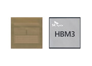
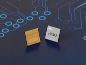
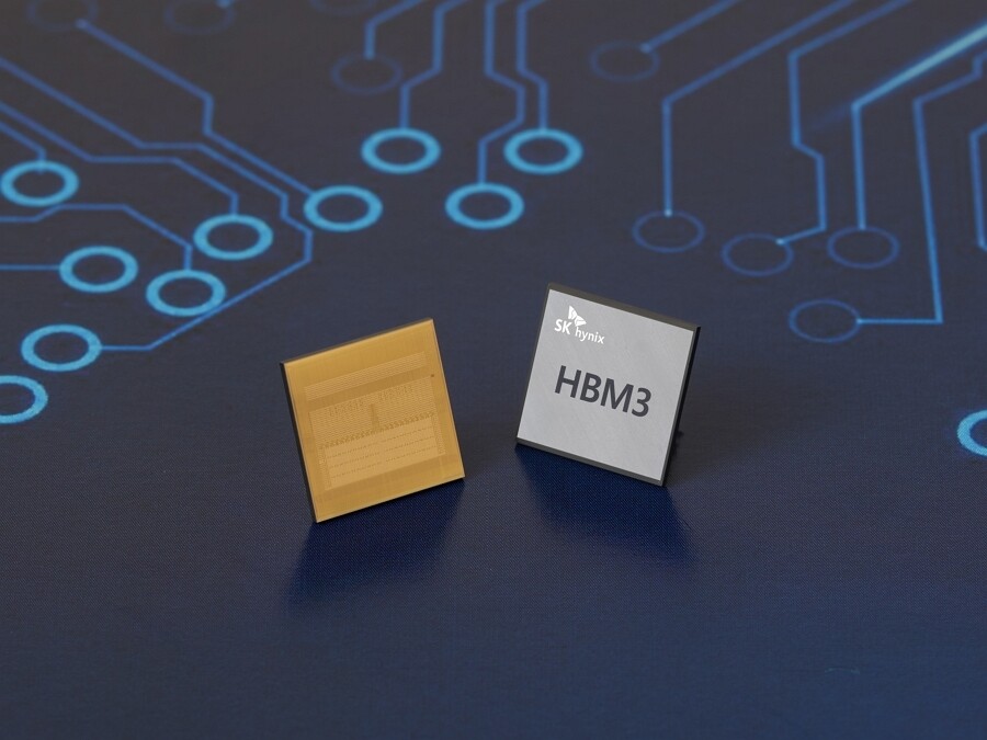
SK hynix Inc. announced that it has become the first in the industry to successfully develop the High Bandwidth Memory 3, the world's best-performing DRAM. HBM3, the fourth generation of the HBM technology with a combination of multiple DRAM chips vertically connected, is a high value product that innovatively raises the data processing rate.

The latest development, which follows the start of mass production of HBM2E in July last year, is expected to help consolidate the company's leadership in the market. SK hynix was also the first in the industry to start mass production of HBM2E. SK hynix's HBM3 is not only the fastest DRAM in the world, but also comes with the biggest capacity and significantly improved level of quality.


The latest product can process up to 819 GB (Gigabyte) per second, meaning that 163 FHD (full-HD) movies (5 GB each) can be transmitted in a single second. This represents a 78% increase in the data-processing speed compared with the HBM2E. It also corrects data (bit) errors with the help of the built-in on-die error-correction code, significantly improving the reliability of the product.

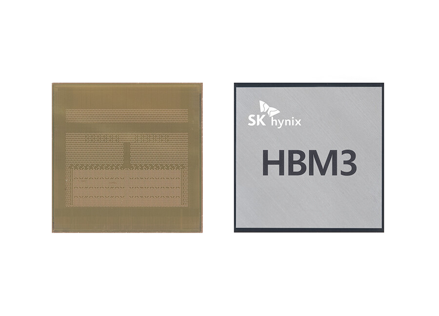
SK hynix's HBM3 will be provided in two capacity types of 24 GB - the industry's biggest -- and 16 GB. For the 24 GB product, SK hynix engineers ground the height of a DRAM chip to approximately 30 micrometer, equivalent to a third of an A4 paper's thickness, before vertically stacking 12 chips using the through silicon via technology.

HBM3 is expected to be mainly adopted by high-performance data centers as well as machine learning platforms that enhance the level of artificial intelligence and super computing performance used to conduct climate change analysis and drug development.

"Since its launch of the world's first HBM DRAM, SK hynix has succeeded in developing the industry's first HBM3 after leading the HBM2E market," said Seon-yong Cha, Executive Vice President in charge of the DRAM development. "We will continue our efforts to solidify our leadership in the premium memory market and help boost the values of our customers by providing products that are in line with the ESG management standards."

View at TechPowerUp Main Site
 
Joined
Dec 17, 2011
Messages
359 (0.08/day)
819 GByte/sec divided by 128 Bytes / cycle = 6400 million cycles per sec = 6400 MHz clock speed
 
Joined
Dec 1, 2020
Messages
360 (0.29/day)
Processor Ryzen 5 7600X
Motherboard ASRock B650M PG Riptide
Cooling Noctua NH-D15
Memory DDR5 6000Mhz CL28 32GB
Video Card(s) Nvidia Geforce RTX 3070 Palit GamingPro OC
Storage Corsair MP600 Force Series Gen.4 1TB
Joined
Dec 28, 2012
Messages
3,478 (0.84/day)
System Name Skunkworks
Processor 5800x3d
Motherboard x570 unify
Cooling Noctua NH-U12A
Memory 32GB 3600 mhz
Video Card(s) asrock 6800xt challenger D
Storage Sabarent rocket 4.0 2TB, MX 500 2TB
Display(s) Asus 1440p144 27"
Case Old arse cooler master 932
Power Supply Corsair 1200w platinum
Mouse *squeak*
Keyboard Some old office thing
Software openSUSE tumbleweed/Mint 21.2
Insane bandwidth... IMAGINE a gpu being feed this amount of data
The last HBM GPU we got was the vega 64, and before that the fury x, neither of which was very impressive.
 
Joined
Dec 17, 2011
Messages
359 (0.08/day)
Insane bandwidth... IMAGINE a gpu being feed this amount of data

NVIDIA GeForce RTX 3090 - 24 GB​

Memory Bandwidth: 936 GB/sec

NVIDIA GeForce RTX 3080 Ti - 12 GB​

Memory Bandwidth: 912 GB/sec

NVIDIA GeForce RTX 3080 - 10 GB​

Memory Bandwidth: 760 GB/sec
 
Last edited:
Joined
Jun 5, 2021
Messages
284 (0.27/day)
The last HBM GPU we got was the vega 64, and before that the fury x, neither of which was very impressive.
Maybe it was the architecture not the memory.. rdna architecture is way better than vega

NVIDIA GeForce RTX 3090 - 24 GB​

Memory Bandwidth: 936 GB/sec

NVIDIA GeForce RTX 3080 Ti - 12 GB​

Memory Bandwidth: 912 GB/sec

NVIDIA GeForce RTX 3080 - 10 GB​

Memory Bandwidth: 760 GB/sec
Gddr6x is horrible its a power pig... hbm is way more efficient if a 3080 had hbm its tdp would be 250 watts
 
Joined
Oct 12, 2005
Messages
682 (0.10/day)
This is the bandwidth for 1 stack. Vega 64 had 2 stack of those. A GPU having the same layout today would have either 32 or 48 GB or VRAM and 1.64 GB/s of bandwidth.

But the main benefits of HBM is having a lower queue latency in high bandwidth situation and lower power per bit transferred.
 
Joined
Jun 3, 2010
Messages
2,540 (0.50/day)
819 GByte/sec divided by 128 Bytes / cycle = 6400 million cycles per sec = 6400 MHz clock speed
Hi,
vertically stacking 12 chips
819 gbps per module = 12 x 1024 bit x _ gbps. It is running at 8333 gbps. There is an error in translation. You cannot have 1 gbps = 1 GB/s. Plus this isn't a 128 bit GDDR bus.

I had to check via Xilinx;
Theoretical Bandwidth = 2x16x64x1800Mbps=3.686Tb/s or 460GB/s
It needs to run at 8533MHz to be close to 819GB/s.
 
Joined
Dec 17, 2011
Messages
359 (0.08/day)
819 gbps per module = 12 x 1024 bit x _ gbps. It is running at 8333 gbps. There is an error in translation. You cannot have 1 gbps = 1 GB/s. Plus this isn't a 128 bit GDDR bus.

1. It doesn't matter how many memory chips a module has - 8 or 12, it makes no difference to the bandwidth. The GPU will see it as a 1024 bits wide and 819 GB/sec.
2. 1 module = 1024 bits wide = 128 bytes wide
3. 819 GigaByte per sec = 128 Byte per Hz * __ GigaHz which gives us 819/128 GHz = 6.4 GHz

Don't take my word for it - https://www.anandtech.com/show/1702...first-hbm3-memory-24gb-stacks-at-up-to-64gbps
 
Joined
Dec 28, 2012
Messages
3,478 (0.84/day)
System Name Skunkworks
Processor 5800x3d
Motherboard x570 unify
Cooling Noctua NH-U12A
Memory 32GB 3600 mhz
Video Card(s) asrock 6800xt challenger D
Storage Sabarent rocket 4.0 2TB, MX 500 2TB
Display(s) Asus 1440p144 27"
Case Old arse cooler master 932
Power Supply Corsair 1200w platinum
Mouse *squeak*
Keyboard Some old office thing
Software openSUSE tumbleweed/Mint 21.2
Maybe it was the architecture not the memory.. rdna architecture is way better than vega
The 1080ti was much faster then the vega 64, and did so using GDDR5 memory. HBM offered absolutely nothing, that bandwidth at that latency really didnt offer much. They also made it much harder for AIBs to make custom heatsink designs.

Gddr6x is horrible its a power pig... hbm is way more efficient if a 3080 had hbm its tdp would be 250 watts
and it would cost another $500 over where it is now. Between the high cost of HBM and the substrate costs went out of control

 
Joined
Jun 3, 2010
Messages
2,540 (0.50/day)
1. It doesn't matter how many memory chips a module has - 8 or 12, it makes no difference to the bandwidth. The GPU will see it as a 1024 bits wide and 819 GB/sec.
2. 1 module = 1024 bits wide = 128 bytes wide
3. 819 GigaByte per sec = 128 Byte per Hz * __ GigaHz which gives us 819/128 GHz = 6.4 GHz

Don't take my word for it - https://www.anandtech.com/show/1702...first-hbm3-memory-24gb-stacks-at-up-to-64gbps
Hi again,
Don't take my word for it, but there are lots of mistranslations going on.
One example:
Each HBM3 memory module is up to 24GB in capacity and can reach a bandwidth of 819Gbps, https://today.in-24.com/technology/482372.html
While I do agree that the io is indeed "1024-bit" wide, it is for 16 channel(16 hi?) stacks which this is not.

I couldn't find a good way to distribute it over 12 layers, so it is all theoretical when it comes to the "16 channel x 64 bit" distribution. What this comes down to is, it will in practice act like a 768-bit interface.
 
Joined
Dec 17, 2011
Messages
359 (0.08/day)
While I do agree that the io is indeed "1024-bit" wide, it is for 16 channel(16 hi?) stacks which this is not.

You only need an 8 Hi stack for 1024 bit wide module. Each memory chip is good for 128 bit width, so with 8 chips you get "8 channel x 128 bit". Having 4 extra (and thus a 12 Hi) stack is only for capacity and not for further increasing the width. 12 Hi stack doesn't mean 1536 bit wide module, its still 1024 bit wide.

I couldn't find a good way to distribute it over 12 layers, so it is all theoretical when it comes to the "16 channel x 64 bit" distribution. What this comes down to is, it will in practice act like a 768-bit interface.

Distributing eight 128 bit channels over 12 memory chips is easy. Say you have to 12 items (A, B, C, D, ... L). Divide each of those 12 items into 8 subitems. I'll call them A1, A2, A3. A4, A5. A5, A6, A7, A8, B1, B2, ....B7, B8 and so on till L1, .... ,L8. You have 48 subitems now. This is how you distribute them between 12 chips -

1634789025699.png


Whenever you want to access any item, you have access 8 channels for max speed. Of course, this is a very simplistic viewpoint. In reality you will have much more than 12 items and some will be small, some large and it will have to be distributed in a complicated manner, but this is the essence of how it will work.

One more thing - you might ask why is it that GDDR6X is only 32 bit wide per memory chip and HBM is 128 bit wide per memory chip and the answer to that is 32 bit and 128 bit are the width of the connection between the memory chip and processor. It is in no way indication of what happens inside the memory chip. What is happening inside the memory chip is beyond my scope of explanation in a forum. GDDR6X is a narrow, fast connection (think 32 traffic lanes but each lane is super fast). HBM is a wider, slower connection (think 128 traffic lanes but each lane is slower).

GDDR6X - narrow 32 bit connection but very fast 21 GHz speed
HBM3 - wider 128 bit connection but slower 6.4 GHz speed

Fun fact - in 2012, AMD and Nvidia were very proud that they achieved 6 GHz speed with 256/384 bit wide bus. 10 years later, in 2022, we will have 2048/4096 bit wide bus operating at 6+ GHz.

Gddr6x is horrible its a power pig... hbm is way more efficient if a 3080 had hbm its tdp would be 250 watts

If 3080 had HBM it would be so expensive that nobody will buy it. What we need is for cards like 3070 Ti and 3080 to have 16 GB and 20 GB memory capacity. it's an atrocity that 3060 has more memory capacity than 3060 Ti, 3070, 3070 Ti and 3080. RTX 3060 has as much memory as the 3080 Ti. If you want more memory than the 3060 can provide you need to go to 3090. This is just stupid.
 
Last edited:
Joined
Jun 3, 2010
Messages
2,540 (0.50/day)
Whenever you want to access any item, you have access 8 channels for max speed. Of course, this is a very simplistic viewpoint.
Yes it is. You are not telling us that 8 channel mode is legacy mode and those gaps are tfaw restriction windows.
I'm not stupid enough to recommend 8 channel mode. Anybody can recommend HBM1 instead of 2 and 3...
 
Top