Report an Error


ATI RV280

RV280
RV280 GL

RV280 9200

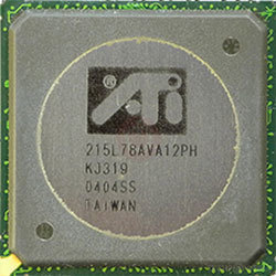
215L78AVA12PH

Die Shot
ATI's RV280 GPU uses the Rage 7 architecture and is made using a 150 nm production process at UMC. With a die size of 98 mm² and a transistor count of 36 million it is a very small chip. RV280 supports DirectX 8.1. Modern GPU compute technologies are not available. It features 4 pixel shaders and 1 vertex shaders, 4 texture mapping units and 4 ROPs. Due to the lack of unified shaders you will not be able to run recent games at all (which require unified shader/DX10+ support).
Graphics Processor
- Released
- Mar 1st, 2003
- GPU Name
- RV280
- Mobile Variant
- M9 / M9+
- Codename
- Argus
- Architecture
- Rage 7
- Foundry
- UMC
- Process Size
- 150 nm
- Transistors
- 36 million
- Density
- 367.3K / mm²
- Die Size
- 98 mm²
Graphics Features
- DirectX
- 8.1
- OpenGL
- 1.4
- OpenCL
- N/A
- Vulkan
- N/A
- Pixel Shader
- 1.4
- Vertex Shader
- 1.1
- Compute
- GFX1
Render Config
- Pixel Shaders
- 4
- Vertex Shaders
- 1
- TMUs
- 4
- ROPs
- 4
- Max. TDP
- 28 W
All Rage 7 GPUs
ATI GPU Architecture History
Graphics cards using the ATI RV280 GPU
| Name | Chip | Memory | Shaders | TMUs | ROPs | GPU Clock | Memory Clock |
|---|---|---|---|---|---|---|---|
| RV280 LX | 64 MB | 4 / 1 | 4 | 4 | 240 MHz | 200 MHz | |
| RV280 9200 SE | 64 MB | 4 / 1 | 4 | 4 | 200 MHz | 166 MHz | |
| 64 MB | 4 / 1 | 4 | 4 | 250 MHz | 200 MHz | ||
| RV280 9200 | 128 MB | 4 / 1 | 4 | 4 | 250 MHz | 200 MHz | |
| RV280 9200 | 128 MB | 4 / 1 | 4 | 4 | 250 MHz | 200 MHz | |
| RV280 9200 SE | 128 MB | 4 / 1 | 4 | 4 | 250 MHz | 164 MHz | |
| 64 MB | 4 / 1 | 4 | 4 | 200 MHz | 166 MHz | ||
| 128 MB | 4 / 1 | 4 | 4 | 250 MHz | 200 MHz | ||
| 128 MB | 4 / 1 | 4 | 4 | 240 MHz | 200 MHz | ||
| RV280 GL | 64 MB | 4 / 1 | 4 | 4 | 240 MHz | 200 MHz | |
| 128 MB | 4 / 1 | 4 | 4 | 240 MHz | 166 MHz |


RV280 GPU Notes
| Mobile Variant: M9 / M9+ Codename: Argus Graphics/Compute: GFX1 Smart Shader 1.0 Smooth Vision 1.0 TruForm 1.0 FullStream Hyper Z II Video Shader Video Immersion II Programmable pixel&vertex pipelines |
Apr 24th, 2024 22:08 EDT
change timezone
Latest GPU Drivers
New Forum Posts
- I am getting artifacting when I change Windows security settings. Is my GPU failing, or is this just a Windows issue? (10)
- Is there a technical reason that Windows 11 doesn't have built into it battery charge limitation? (42)
- (Anti) SFF fun house (347)
- Cinebench crashed my PC. My Wi-Fi stopped working, and I keep getting a "Please wait" screen when I boot up my PC. (30)
- The TPU UK Clubhouse (24783)
- Sharing experience with MSI RTX 3070 vBIOS update to enable Resizable Bar with MB Z490 (2)
- Share your AIDA 64 cache and memory benchmark here (2915)
- Will a RTX 4070 TI super bottleneck a Ryzen 9 7950X3D? (58)
- The best *budget* ATX PC case on the market? (24)
- GTX 1070 Ti - TDP Issues - Always Power Throttling (4)
Popular Reviews
- Fractal Design Terra Review
- Thermalright Phantom Spirit 120 EVO Review
- Corsair 2000D Airflow Review
- Minisforum EliteMini UM780 XTX (AMD Ryzen 7 7840HS) Review
- ASUS GeForce RTX 4090 STRIX OC Review
- NVIDIA GeForce RTX 4090 Founders Edition Review - Impressive Performance
- ASUS GeForce RTX 4090 Matrix Platinum Review - The RTX 4090 Ti
- MSI GeForce RTX 4090 Suprim X Review
- Gigabyte GeForce RTX 4090 Gaming OC Review
- MSI GeForce RTX 4090 Gaming X Trio Review
Controversial News Posts
- Sony PlayStation 5 Pro Specifications Confirmed, Console Arrives Before Holidays (116)
- NVIDIA Points Intel Raptor Lake CPU Users to Get Help from Intel Amid System Instability Issues (106)
- AMD "Strix Halo" Zen 5 Mobile Processor Pictured: Chiplet-based, Uses 256-bit LPDDR5X (101)
- US Government Wants Nuclear Plants to Offload AI Data Center Expansion (98)
- Windows 10 Security Updates to Cost $61 After 2025, $427 by 2028 (84)
- Developers of Outpost Infinity Siege Recommend Underclocking i9-13900K and i9-14900K for Stability on Machines with RTX 4090 (84)
- TechPowerUp Hiring: Reviewers Wanted for Motherboards, Laptops, Gaming Handhelds and Prebuilt Desktops (78)
- AMD's RDNA 4 GPUs Could Stick with 18 Gbps GDDR6 Memory (73)