Report an Error


NVIDIA NV15

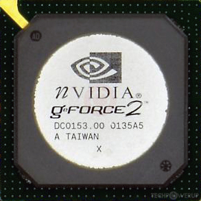
NV15

GeForce2 GTS

GeForce2 GTS PRO

GeForce2 PRO

GeForce2 Ti
GeForce2 Ultra

NV15GL A4

Oleg Kashirin
Die Shot
NVIDIA's NV15 GPU uses the Celsius architecture and is made using a 180 nm production process at TSMC. With a die size of 88 mm² and a transistor count of 25 million it is a very small chip. NV15 supports DirectX 7.0. Modern GPU compute technologies are not available. It features 4 pixel shaders and 0 vertex shaders, 8 texture mapping units and 4 ROPs. Due to the lack of unified shaders you will not be able to run recent games at all (which require unified shader/DX10+ support).
Graphics Processor
- Released
- Apr 26th, 2000
- GPU Name
- NV15
- Architecture
- Celsius
- Foundry
- TSMC
- Process Size
- 180 nm
- Transistors
- 25 million
- Density
- 284.1K / mm²
- Die Size
- 88 mm²
Graphics Features
- DirectX
- 7.0
- OpenGL
- 1.5
- OpenCL
- N/A
- Vulkan
- N/A
- Pixel Shader
- 0.5
- Vertex Shader
- N/A
Render Config
- Pixel Shaders
- 4
- Vertex Shaders
- 0
- TMUs
- 8
- ROPs
- 4
All Celsius GPUs
NVIDIA GPU Architecture History
- 2023 Hopper
- 2022-2024 Ada Lovelace
- 2020-2024 Ampere
- 2018-2022 Turing
- 2017-2020 Volta
- 2016-2021 Pascal
- 2014-2019 Maxwell 2.0
- 2014-2017 Maxwell
- 2013-2015 Kepler 2.0
- 2012-2018 Kepler
- 2010-2016 Fermi 2.0
- 2010-2013 VLIW Vec4
- 2010-2016 Fermi
- 2007-2013 Tesla 2.0
- 2006-2010 Tesla
- 2003-2013 Curie
- 2003-2005 Rankine
- 2001-2003 Kelvin
- 1999-2005 Celsius
- 1998-2000 Fahrenheit
Graphics cards using the NVIDIA NV15 GPU
| Name | Chip | Memory | Shaders | TMUs | ROPs | GPU Clock | Memory Clock |
|---|---|---|---|---|---|---|---|
| GeForce2 Ultra | 64 MB | 4 / 0 | 8 | 4 | 250 MHz | 230 MHz | |
| GeForce2 Ti | 64 MB | 4 / 0 | 8 | 4 | 250 MHz | 200 MHz | |
| GeForce2 PRO | 64 MB | 4 / 0 | 8 | 4 | 200 MHz | 200 MHz | |
| GeForce2 GTS | 32 MB | 4 / 0 | 8 | 4 | 200 MHz | 166 MHz | |
| GeForce2 GTS PRO | 32 MB | 4 / 0 | 8 | 4 | 200 MHz | 200 MHz | |
| NV15GL A4 | 64 MB | 4 / 0 | 8 | 4 | 200 MHz | 250 MHz |


Apr 24th, 2024 05:14 EDT
change timezone
Latest GPU Drivers
New Forum Posts
- What phone you use as your daily driver? And, a discussion of them. (1458)
- What's your latest tech purchase? (20329)
- Which new games will you be buying? (309)
- Official Board Game Discussion (15)
- The TPU UK Clubhouse (24775)
- Serious bug in PHP reported! (3)
- ThrottleStop 9.6 Voltage won't change (2)
- Sexy Mechanical Keyboard Thread (486)
- Is there a technical reason that Windows 11 doesn't have built into it battery charge limitation? (38)
- ROG Strix LC III 360 ARG AIO What should the pump speed be? (3)
Popular Reviews
- Fractal Design Terra Review
- Corsair 2000D Airflow Review
- Thermalright Phantom Spirit 120 EVO Review
- Minisforum EliteMini UM780 XTX (AMD Ryzen 7 7840HS) Review
- ASUS GeForce RTX 4090 STRIX OC Review
- NVIDIA GeForce RTX 4090 Founders Edition Review - Impressive Performance
- ASUS GeForce RTX 4090 Matrix Platinum Review - The RTX 4090 Ti
- MSI GeForce RTX 4090 Suprim X Review
- MSI GeForce RTX 4090 Gaming X Trio Review
- Gigabyte GeForce RTX 4090 Gaming OC Review
Controversial News Posts
- Sony PlayStation 5 Pro Specifications Confirmed, Console Arrives Before Holidays (116)
- NVIDIA Points Intel Raptor Lake CPU Users to Get Help from Intel Amid System Instability Issues (106)
- AMD "Strix Halo" Zen 5 Mobile Processor Pictured: Chiplet-based, Uses 256-bit LPDDR5X (101)
- US Government Wants Nuclear Plants to Offload AI Data Center Expansion (98)
- Windows 10 Security Updates to Cost $61 After 2025, $427 by 2028 (84)
- Developers of Outpost Infinity Siege Recommend Underclocking i9-13900K and i9-14900K for Stability on Machines with RTX 4090 (84)
- TechPowerUp Hiring: Reviewers Wanted for Motherboards, Laptops, Gaming Handhelds and Prebuilt Desktops (77)
- Intel Realizes the Only Way to Save x86 is to Democratize it, Reopens x86 IP Licensing (70)