Report an Error


ATI RV790

RV790
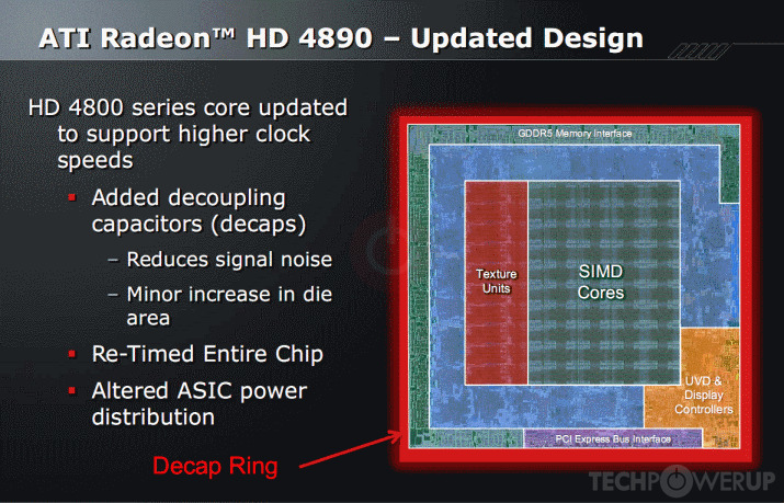
Die Diagram
ATI's RV790 GPU uses the TeraScale architecture and is made using a 55 nm production process at TSMC. With a die size of 282 mm² and a transistor count of 959 million it is a medium-sized chip. RV790 supports DirectX 10.1 (Feature Level 10_1). For GPU compute applications, OpenCL version 1.1 can be used. It features 800 shading units, 40 texture mapping units and 16 ROPs.
Further reading:
R700 Series Instruction Set Architecture 
Graphics Processor
- Released
- Apr 2nd, 2009
- GPU Name
- RV790
- Codename
- Wekiva Plus
- Alt. Codename
- Spartan
- Architecture
- TeraScale
- Foundry
- TSMC
- Process Size
- 55 nm
- Transistors
- 959 million
- Density
- 3.4M / mm²
- Die Size
- 282 mm²
Graphics Features
- DirectX
- 10.1 (10_1)
- OpenGL
- 3.3
- OpenCL
- 1.1
- Vulkan
- N/A
- Shader Model
- 4.1
- WDDM
- 1.1
- Compute
- GFX3
- DCE
- 3.1
- UVD
- 2.0
Render Config
- Shading Units
- 800
- TMUs
- 40
- ROPs
- 16
- Compute Units
- 10
- Z-Stencil
- 64
- L1 Cache
- 16 KB per CU
- L2 Cache
- 256 KB
- Max. TDP
- 190 W
All TeraScale GPUs
- ATI M72
- ATI M74
- ATI M76
- ATI M82
- ATI M84
- ATI M86
- ATI M88
- ATI M92
- AMD M93
- ATI M93
- ATI M96
- ATI M97
- ATI M98
- ATI R600
- ATI R680
- ATI R700
- ATI RS780
- ATI RS880
- ATI RV610
- ATI RV620
- ATI RV630
- ATI RV635
- ATI RV670
- AMD RV670
- ATI RV710
- AMD RV711
- ATI RV711
- ATI RV730
- ATI RV740
- ATI RV770
- AMD RV770
- ATI RV790
- ATI RX881
- ATI Theater 650 PRO
- ATI Xenos Corona
- ATI Xenos Falcon
- ATI Xenos Jasper
- ATI Xenos Vejle
- ATI Xenos Xenon
ATI GPU Architecture History
Graphics cards using the ATI RV790 GPU
| Name | Chip | Memory | Shaders | TMUs | ROPs | GPU Clock | Memory Clock |
|---|---|---|---|---|---|---|---|
| RV790 XT | 1024 MB | 800 | 40 | 16 | 850 MHz | 975 MHz | |
| RV790 GT | 512 MB | 640 | 32 | 16 | 700 MHz | 750 MHz |


RV790 GPU Notes
| Codename: Wekiva Plus (Spartan) Graphics/Compute: GFX3 Display Core Engine: 3.1 Unified Video Decoder: 2.0 |
Apr 24th, 2024 21:43 EDT
change timezone
Latest GPU Drivers
New Forum Posts
- Is there a technical reason that Windows 11 doesn't have built into it battery charge limitation? (42)
- (Anti) SFF fun house (347)
- Cinebench crashed my PC. My Wi-Fi stopped working, and I keep getting a "Please wait" screen when I boot up my PC. (30)
- The TPU UK Clubhouse (24783)
- Sharing experience with MSI RTX 3070 vBIOS update to enable Resizable Bar with MB Z490 (2)
- Share your AIDA 64 cache and memory benchmark here (2915)
- Will a RTX 4070 TI super bottleneck a Ryzen 9 7950X3D? (58)
- The best *budget* ATX PC case on the market? (24)
- GTX 1070 Ti - TDP Issues - Always Power Throttling (4)
- 2022-X58/1366 PIN Motherboards NVME M.2 SSD BIOS MOD Collection (656)
Popular Reviews
- Fractal Design Terra Review
- Thermalright Phantom Spirit 120 EVO Review
- Corsair 2000D Airflow Review
- Minisforum EliteMini UM780 XTX (AMD Ryzen 7 7840HS) Review
- ASUS GeForce RTX 4090 STRIX OC Review
- NVIDIA GeForce RTX 4090 Founders Edition Review - Impressive Performance
- ASUS GeForce RTX 4090 Matrix Platinum Review - The RTX 4090 Ti
- MSI GeForce RTX 4090 Suprim X Review
- MSI GeForce RTX 4090 Gaming X Trio Review
- Gigabyte GeForce RTX 4090 Gaming OC Review
Controversial News Posts
- Sony PlayStation 5 Pro Specifications Confirmed, Console Arrives Before Holidays (116)
- NVIDIA Points Intel Raptor Lake CPU Users to Get Help from Intel Amid System Instability Issues (106)
- AMD "Strix Halo" Zen 5 Mobile Processor Pictured: Chiplet-based, Uses 256-bit LPDDR5X (101)
- US Government Wants Nuclear Plants to Offload AI Data Center Expansion (98)
- Windows 10 Security Updates to Cost $61 After 2025, $427 by 2028 (84)
- Developers of Outpost Infinity Siege Recommend Underclocking i9-13900K and i9-14900K for Stability on Machines with RTX 4090 (84)
- TechPowerUp Hiring: Reviewers Wanted for Motherboards, Laptops, Gaming Handhelds and Prebuilt Desktops (78)
- AMD's RDNA 4 GPUs Could Stick with 18 Gbps GDDR6 Memory (73)