Report an Error


ATI R580

R580

R580 XT

Oleg Kashirin
Die Shot
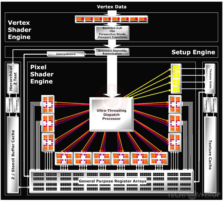
Block Diagram
ATI's R580 GPU uses the Ultra-Threaded SE architecture and is made using a 90 nm production process at TSMC. With a die size of 352 mm² and a transistor count of 384 million it is a large chip. R580 supports DirectX 9.0c (Feature Level 9_3). Modern GPU compute technologies are not available. It features 48 pixel shaders and 8 vertex shaders, 16 texture mapping units and 16 ROPs. Due to the lack of unified shaders you will not be able to run recent games at all (which require unified shader/DX10+ support).
Graphics Processor
- Released
- Jan 13th, 2006
- GPU Name
- R580
- Codename
- Rodin
- Architecture
- Ultra-Threaded SE
- Foundry
- TSMC
- Process Size
- 90 nm
- Transistors
- 384 million
- Density
- 1.1M / mm²
- Die Size
- 352 mm²
Graphics Features
- DirectX
- 9.0c (9_3)
- OpenGL
-
2.1 (full)
3.0 (partial)
- OpenCL
- N/A
- Vulkan
- N/A
- Shader Model
- 3.0
- WDDM
- 1.0
- Compute
- GFX2
- DCE
- 1.0
Render Config
- Pixel Shaders
- 48
- Vertex Shaders
- 8
- TMUs
- 16
- ROPs
- 16
- Max. TDP
- 135 W
All Ultra-Threaded SE GPUs
ATI GPU Architecture History
Graphics cards using the ATI R580 GPU
| Name | Chip | Memory | Shaders | TMUs | ROPs | GPU Clock | Memory Clock |
|---|---|---|---|---|---|---|---|
| R580 XT | 512 MB | 48 / 8 | 16 | 16 | 650 MHz | 775 MHz | |
| R580 AIW | 256 MB | 48 / 8 | 16 | 16 | 500 MHz | 477 MHz | |
| R580 XL | 256 MB | 36 / 8 | 12 | 12 | 575 MHz | 600 MHz | |
| R580 XT | 256 MB | 48 / 8 | 16 | 16 | 625 MHz | 725 MHz | |
| R580 CF | 512 MB | 48 / 8 | 16 | 16 | 625 MHz | 725 MHz | |
| R580 XL | 256 MB | 36 / 8 | 12 | 12 | 575 MHz | 600 MHz |


R580 GPU Notes
| Codename: Rodin Graphics/Compute: GFX2 Display Core Engine: 1.0 Avivo Video Programmable pixel&vertex pipelines |
Apr 19th, 2024 00:54 EDT
change timezone
Latest GPU Drivers
New Forum Posts
- DDR5 RAM Speeds and the future (44)
- What's your latest tech purchase? (20281)
- Should the CDPR make the Fallout 5 instead? (22)
- Cinebench crashed my PC. My Wi-Fi stopped working, and I keep getting a "Please wait" screen when I boot up my PC. (7)
- Adventure: Running 8/9th gen Coffee Lake CPUs on Z170 motherboard (ASUS Maximus VIII Ranger) (336)
- First computer build for my son (1)
- Linus watercools (8)
- Why is SteamOS taking so long to come to desktop for AMD users, when ChimeraOS is the same thing almost? (19)
- Do you use Linux? (229)
- Its time (48)
Popular Reviews
- Horizon Forbidden West Performance Benchmark Review - 30 GPUs Tested
- PowerColor Radeon RX 7900 GRE Hellhound Review
- Fractal Design Terra Review
- Corsair 2000D Airflow Review
- Minisforum EliteMini UM780 XTX (AMD Ryzen 7 7840HS) Review
- Thermalright Phantom Spirit 120 EVO Review
- Creative Pebble X Plus Review
- FiiO KB3 HiFi Mechanical Keyboard Review - Integrated DAC/Amp!
- ASUS GeForce RTX 4090 STRIX OC Review
- NVIDIA GeForce RTX 4090 Founders Edition Review - Impressive Performance
Controversial News Posts
- Sony PlayStation 5 Pro Specifications Confirmed, Console Arrives Before Holidays (109)
- NVIDIA Points Intel Raptor Lake CPU Users to Get Help from Intel Amid System Instability Issues (102)
- US Government Wants Nuclear Plants to Offload AI Data Center Expansion (98)
- Windows 10 Security Updates to Cost $61 After 2025, $427 by 2028 (82)
- Developers of Outpost Infinity Siege Recommend Underclocking i9-13900K and i9-14900K for Stability on Machines with RTX 4090 (82)
- TechPowerUp Hiring: Reviewers Wanted for Motherboards, Laptops, Gaming Handhelds and Prebuilt Desktops (71)
- Intel Realizes the Only Way to Save x86 is to Democratize it, Reopens x86 IP Licensing (70)
- AMD Zen 5 Execution Engine Leaked, Features True 512-bit FPU (63)