Report an Error


ATI RV610
RV610

RV610 LE

Shane Phillips
Die Shot
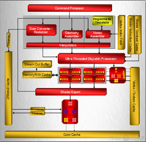
Block Diagram
ATI's RV610 GPU uses the TeraScale architecture and is made using a 65 nm production process at TSMC. With a die size of 85 mm² and a transistor count of 180 million it is a very small chip. RV610 supports DirectX 10.0 (Feature Level 10_0). For GPU compute applications, OpenCL version N/A can be used. It features 40 shading units, 4 texture mapping units and 4 ROPs.
Further reading:
R600 Series Instruction Set Architecture 
Graphics Processor
- Released
- 2007
- GPU Name
- RV610
- Mobile Variant
- M72 / M74
- Codename
- Laka
- Architecture
- TeraScale
- Foundry
- TSMC
- Process Size
- 65 nm
- Transistors
- 180 million
- Density
- 2.1M / mm²
- Die Size
- 85 mm²
- Package
- FCBGA-632
Graphics Features
- DirectX
- 10.0 (10_0)
- OpenGL
- 3.3
- OpenCL
- N/A
- Vulkan
- N/A
- Shader Model
- 4.0
- WDDM
- 1.1
- Compute
- GFX3
- DCE
- 2.0
- UVD
- 1.0
Render Config
- Shading Units
- 40
- TMUs
- 4
- ROPs
- 4
- Compute Units
- 2
- Vertex Cache
- 32 KB
- Texture Cache
- 32 KB
- Tex L1 Cache
- 32 KB per 4 SPs
- L2 Cache
- 32 KB
- Max. TDP
- 25 W
All TeraScale GPUs
- ATI M72
- ATI M74
- ATI M76
- ATI M82
- ATI M84
- ATI M86
- ATI M88
- ATI M92
- AMD M93
- ATI M93
- ATI M96
- ATI M97
- ATI M98
- ATI R600
- ATI R680
- ATI R700
- ATI RS780
- ATI RS880
- ATI RV610
- ATI RV620
- ATI RV630
- ATI RV635
- ATI RV670
- AMD RV670
- ATI RV710
- AMD RV711
- ATI RV711
- ATI RV730
- ATI RV740
- ATI RV770
- AMD RV770
- ATI RV790
- ATI RX881
- ATI Theater 650 PRO
- ATI Xenos Corona
- ATI Xenos Falcon
- ATI Xenos Jasper
- ATI Xenos Vejle
- ATI Xenos Xenon
ATI GPU Architecture History
Graphics cards using the ATI RV610 GPU
| Name | Chip | Memory | Shaders | TMUs | ROPs | GPU Clock | Memory Clock |
|---|---|---|---|---|---|---|---|
| RV610 PRO | 256 MB | 40 | 4 | 4 | 650 MHz | 500 MHz | |
| 256 MB | 40 | 4 | 4 | 525 MHz | 400 MHz | ||
| RV610 LE | 512 MB | 40 | 4 | 4 | 525 MHz | 400 MHz | |
| RV610 LE AGP | 256 MB | 40 | 4 | 4 | 525 MHz | 400 MHz | |
| RV610 LE | 256 MB | 40 | 4 | 4 | 525 MHz | 400 MHz | |
| E2400 | 128 MB | 40 | 4 | 4 | 600 MHz | 700 MHz | |
| 256 MB | 40 | 4 | 4 | 519 MHz | 396 MHz | ||
| 256 MB | 40 | 4 | 4 | 398 MHz | 495 MHz |


RV610 GPU Notes
| Mobile Variant: M72 / M74 Codename: Laka Graphics/Compute: GFX3 Display Core Engine: 2.0 Unified Video Decoder: 1.0 |
Apr 19th, 2024 22:57 EDT
change timezone
Latest GPU Drivers
New Forum Posts
- GPU-Z reporting wrong ReBar info for RTX 20 series (3)
- I just succesfully baked DDR4 (74)
- Official Board Game Discussion (4)
- Roccat Kone AIMO has developed a double left click, when I click it once. Any fix out there? (37)
- Cinebench crashed my PC. My Wi-Fi stopped working, and I keep getting a "Please wait" screen when I boot up my PC. (8)
- USB C to USB A hub (43)
- XFX RX580 stock Bios (8)
- Your PC ATM (34488)
- 2 questions about Oculus Quest 3 (0)
- Liquidextasy waterblocks (50)
Popular Reviews
- Horizon Forbidden West Performance Benchmark Review - 30 GPUs Tested
- Fractal Design Terra Review
- Corsair 2000D Airflow Review
- Thermalright Phantom Spirit 120 EVO Review
- Minisforum EliteMini UM780 XTX (AMD Ryzen 7 7840HS) Review
- Creative Pebble X Plus Review
- FiiO KB3 HiFi Mechanical Keyboard Review - Integrated DAC/Amp!
- ASUS GeForce RTX 4090 STRIX OC Review
- NVIDIA GeForce RTX 4090 Founders Edition Review - Impressive Performance
- ASUS GeForce RTX 4090 Matrix Platinum Review - The RTX 4090 Ti
Controversial News Posts
- Sony PlayStation 5 Pro Specifications Confirmed, Console Arrives Before Holidays (111)
- NVIDIA Points Intel Raptor Lake CPU Users to Get Help from Intel Amid System Instability Issues (102)
- US Government Wants Nuclear Plants to Offload AI Data Center Expansion (98)
- AMD "Strix Halo" Zen 5 Mobile Processor Pictured: Chiplet-based, Uses 256-bit LPDDR5X (84)
- Windows 10 Security Updates to Cost $61 After 2025, $427 by 2028 (82)
- Developers of Outpost Infinity Siege Recommend Underclocking i9-13900K and i9-14900K for Stability on Machines with RTX 4090 (82)
- TechPowerUp Hiring: Reviewers Wanted for Motherboards, Laptops, Gaming Handhelds and Prebuilt Desktops (72)
- Intel Realizes the Only Way to Save x86 is to Democratize it, Reopens x86 IP Licensing (70)