Report an Error


AMD Barts

Barts

Barts XT
Shane Phillips
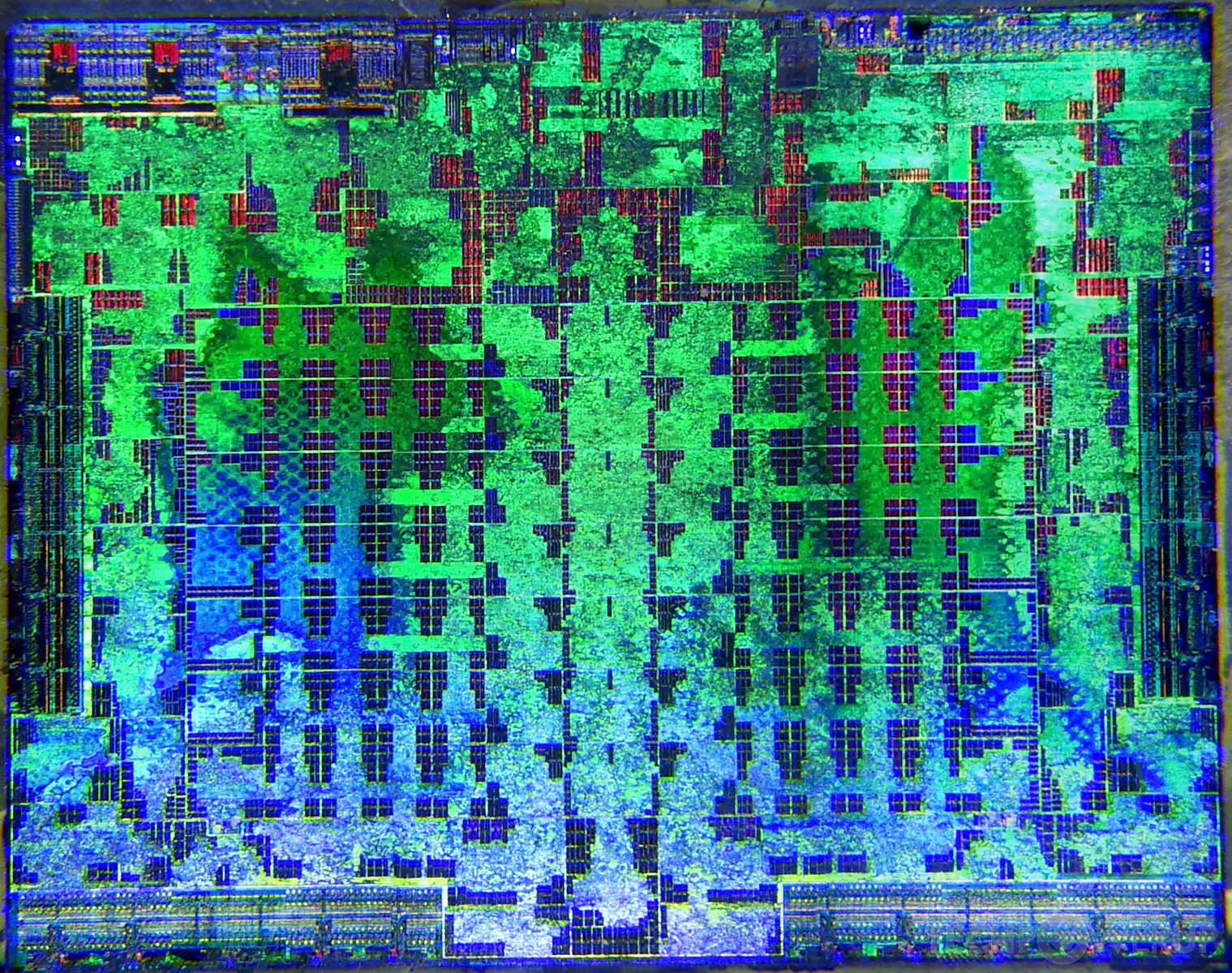
Die Shot

Block Diagram

Information

Information 2
AMD's Barts GPU uses the TeraScale 2 architecture and is made using a 40 nm production process at TSMC. With a die size of 255 mm² and a transistor count of 1,700 million it is a medium-sized chip. Barts supports DirectX 11.2 (Feature Level 11_0). For GPU compute applications, OpenCL version 1.2 can be used. It features 1120 shading units, 56 texture mapping units and 32 ROPs.
Further reading:
TeraScale 2 Instruction Set Architecture 
Graphics Processor
- Released
- Oct 21st, 2010
- GPU Name
- Barts
- Mobile Variant
- Blackcomb
- Codename
- Victoria
- Generation
- Northern Islands
- Architecture
- TeraScale 2
- Foundry
- TSMC
- Process Size
- 40 nm
- Transistors
- 1,700 million
- Density
- 6.7M / mm²
- Die Size
- 255 mm²
- Package
- HFCBGA-1737
Graphics Features
- DirectX
- 11.2 (11_0)
- OpenGL
- 4.4
- OpenCL
- 1.2
- Vulkan
- N/A
- Shader Model
- 5.0
- WDDM
- 1.3
- Compute
- GFX4
- DCE
- 5.0
- UVD
- 3.1
Render Config
- Shading Units
- 1120
- TMUs
- 56
- ROPs
- 32
- Compute Units
- 14
- Z-Stencil
- 40
- L1 Cache
- 8 KB per CU
- L2 Cache
- 512 KB
- Max. TDP
- 300 W
All TeraScale 2 GPUs
- AMD Barts
- AMD Blackcomb
- ATI Broadway
- AMD Broadway
- AMD Caicos
- AMD Capilano
- ATI Cedar
- AMD Cedar
- ATI Cypress
- AMD Cypress
- AMD Granville
- ATI Hemlock
- AMD Juniper
- ATI Juniper
- AMD Latte
- AMD Lexington
- AMD Loveland
- ATI Madison
- AMD Onega
- ATI Park
- AMD Park
- ATI Pinewood
- AMD Pinewood
- ATI Redwood
- AMD Redwood
- AMD Robson
- AMD Seymour
- AMD Sumo
- AMD SuperSumo
- AMD Thames
- AMD Turks
- ATI Turks
- AMD Whistler
AMD GPU Architecture History
Graphics cards using the AMD Barts GPU
| Name | Chip | Memory | Shaders | TMUs | ROPs | GPU Clock | Memory Clock |
|---|---|---|---|---|---|---|---|
| Barts PRO | 1024 MB | 960 | 48 | 32 | 775 MHz | 1000 MHz | |
| Barts XT | 1024 MB | 1120 | 56 | 32 | 900 MHz | 1050 MHz | |
| Barts LE | 1024 MB | 800 | 40 | 16 | 840 MHz | 1050 MHz | |
| Barts XT | 1024 MB | 1120 | 56 | 32 | 900 MHz | 1050 MHz | |
| Barts PRO | 2 GB | 960 | 48 | 32 | 800 MHz | 1050 MHz | |
| Barts LE | 1024 MB | 800 | 40 | 32 | 840 MHz | 1050 MHz |


Barts GPU Notes
| Generation: Northern Islands Mobile Variant: Blackcomb Codename: Victoria Graphics/Compute: GFX4 Display Core Engine: 5.0 Unified Video Decoder: 3.1 |
Apr 19th, 2024 19:58 EDT
change timezone
Latest GPU Drivers
New Forum Posts
- AMD RX 7000 series GPU Owners' Club (1068)
- I just succesfully baked DDR4 (69)
- I9 13890HX undervolting Suggestions (4)
- Undervolting Dell XPS 14 9440 is it possible? (7)
- Share your AIDA 64 cache and memory benchmark here (2884)
- Roccat Kone AIMO has developed a double left click, when I click it once. Any fix out there? (34)
- The TPU UK Clubhouse (24738)
- XFX RX580 stock Bios (7)
- Looks like the Z80 is finished (2)
- AAF Optimus DCH Audio Modded Driver for Windows 10/11 - For ALL HDAUDIO Enumerator Chips (642)
Popular Reviews
- Horizon Forbidden West Performance Benchmark Review - 30 GPUs Tested
- PowerColor Radeon RX 7900 GRE Hellhound Review
- Fractal Design Terra Review
- Corsair 2000D Airflow Review
- Thermalright Phantom Spirit 120 EVO Review
- Minisforum EliteMini UM780 XTX (AMD Ryzen 7 7840HS) Review
- Creative Pebble X Plus Review
- FiiO KB3 HiFi Mechanical Keyboard Review - Integrated DAC/Amp!
- ASUS GeForce RTX 4090 STRIX OC Review
- NVIDIA GeForce RTX 4090 Founders Edition Review - Impressive Performance
Controversial News Posts
- Sony PlayStation 5 Pro Specifications Confirmed, Console Arrives Before Holidays (111)
- NVIDIA Points Intel Raptor Lake CPU Users to Get Help from Intel Amid System Instability Issues (102)
- US Government Wants Nuclear Plants to Offload AI Data Center Expansion (98)
- AMD "Strix Halo" Zen 5 Mobile Processor Pictured: Chiplet-based, Uses 256-bit LPDDR5X (83)
- Windows 10 Security Updates to Cost $61 After 2025, $427 by 2028 (82)
- Developers of Outpost Infinity Siege Recommend Underclocking i9-13900K and i9-14900K for Stability on Machines with RTX 4090 (82)
- TechPowerUp Hiring: Reviewers Wanted for Motherboards, Laptops, Gaming Handhelds and Prebuilt Desktops (72)
- Intel Realizes the Only Way to Save x86 is to Democratize it, Reopens x86 IP Licensing (70)