Report an Error


NVIDIA GF116

GF116

GF116-110-KA-A1
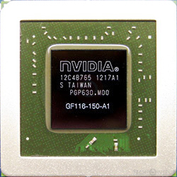
GF116-150-A1

GF116-200-KA-A1

Block Diagram

SM Diagram
NVIDIA's GF116 GPU uses the Fermi 2.0 architecture and is made using a 40 nm production process at TSMC. With a die size of 238 mm² and a transistor count of 1,170 million it is a medium-sized chip. GF116 supports DirectX 12 (Feature Level 11_0). For GPU compute applications, OpenCL version 1.1 and CUDA 2.1 can be used. It features 192 shading units, 32 texture mapping units and 24 ROPs.
Further reading:
Fermi Compute Architecture 
Graphics Processor
- Released
- Mar 15th, 2011
- GPU Name
- GF116
- Codename
- NVCF
- Architecture
- Fermi 2.0
- Foundry
- TSMC
- Process Size
- 40 nm
- Transistors
- 1,170 million
- Density
- 4.9M / mm²
- Die Size
- 238 mm²
- Package
- BGA-1337
Graphics Features
- DirectX
- 12 (11_0)
- OpenGL
- 4.6
- OpenCL
- 1.1
- Vulkan
- N/A
- CUDA
- 2.1
- Shader Model
- 5.1
- WDDM
- 2.3
- PureVideo HD
- VP4
- VDPAU
- Feature Set C
Render Config
- Shading Units
- 192
- TMUs
- 32
- ROPs
- 24
- SM Count
- 4
- SFUs
- 32
- GPCs
- 1
- L1 Cache
- 64 KB per SM
- L2 Cache
- 384 KB
- Max. TDP
- 116 W
All Fermi 2.0 GPUs
NVIDIA GPU Architecture History
- 2023 Hopper
- 2022-2024 Ada Lovelace
- 2020-2024 Ampere
- 2018-2022 Turing
- 2017-2020 Volta
- 2016-2021 Pascal
- 2014-2019 Maxwell 2.0
- 2014-2017 Maxwell
- 2013-2015 Kepler 2.0
- 2012-2018 Kepler
- 2010-2016 Fermi 2.0
- 2010-2013 VLIW Vec4
- 2010-2016 Fermi
- 2007-2013 Tesla 2.0
- 2006-2010 Tesla
- 2003-2013 Curie
- 2003-2005 Rankine
- 2001-2003 Kelvin
- 1999-2005 Celsius
- 1998-2000 Fahrenheit
Graphics cards using the NVIDIA GF116 GPU
| Name | Chip | Memory | Shaders | TMUs | ROPs | GPU Clock | Memory Clock |
|---|---|---|---|---|---|---|---|
| GF116-400-A1 | 1024 MB | 192 | 32 | 24 | 900 MHz | 1026 MHz | |
| GF116-200-KA-A1 | 1024 MB | 192 | 32 | 16 | 783 MHz | 902 MHz | |
| GF116-110-KA-A1 | 1024 MB | 144 | 24 | 16 | 871 MHz | 1000 MHz | |
| 1536 MB | 144 | 24 | 16 | 720 MHz | 800 MHz | ||
| GF116-150-A1 | 1536 MB | 144 | 24 | 24 | 720 MHz | 800 MHz | |
| N12E-GS-A1 | 1536 MB | 192 | 32 | 24 | 775 MHz | 625 MHz | |
| GF116-200-KA-A1 | 1024 MB | 144 | 24 | 16 | 783 MHz | 700 MHz | |
| 1024 MB | 144 | 24 | 16 | 475 MHz | 900 MHz |


GF116 GPU Notes
| PureVideo HD: VP4 VDPAU: Feature Set C |
Apr 19th, 2024 20:12 EDT
change timezone
Latest GPU Drivers
New Forum Posts
- GTX 1060 6GB ASUS GPU Shuts Down after 5min of Gaming (0)
- AMD RX 7000 series GPU Owners' Club (1068)
- I just succesfully baked DDR4 (69)
- I9 13890HX undervolting Suggestions (4)
- Undervolting Dell XPS 14 9440 is it possible? (7)
- Share your AIDA 64 cache and memory benchmark here (2884)
- Roccat Kone AIMO has developed a double left click, when I click it once. Any fix out there? (34)
- The TPU UK Clubhouse (24738)
- XFX RX580 stock Bios (7)
- Looks like the Z80 is finished (2)
Popular Reviews
- Horizon Forbidden West Performance Benchmark Review - 30 GPUs Tested
- Fractal Design Terra Review
- Corsair 2000D Airflow Review
- Thermalright Phantom Spirit 120 EVO Review
- Minisforum EliteMini UM780 XTX (AMD Ryzen 7 7840HS) Review
- Creative Pebble X Plus Review
- FiiO KB3 HiFi Mechanical Keyboard Review - Integrated DAC/Amp!
- ASUS GeForce RTX 4090 STRIX OC Review
- NVIDIA GeForce RTX 4090 Founders Edition Review - Impressive Performance
- ASUS GeForce RTX 4090 Matrix Platinum Review - The RTX 4090 Ti
Controversial News Posts
- Sony PlayStation 5 Pro Specifications Confirmed, Console Arrives Before Holidays (111)
- NVIDIA Points Intel Raptor Lake CPU Users to Get Help from Intel Amid System Instability Issues (102)
- US Government Wants Nuclear Plants to Offload AI Data Center Expansion (98)
- AMD "Strix Halo" Zen 5 Mobile Processor Pictured: Chiplet-based, Uses 256-bit LPDDR5X (84)
- Windows 10 Security Updates to Cost $61 After 2025, $427 by 2028 (82)
- Developers of Outpost Infinity Siege Recommend Underclocking i9-13900K and i9-14900K for Stability on Machines with RTX 4090 (82)
- TechPowerUp Hiring: Reviewers Wanted for Motherboards, Laptops, Gaming Handhelds and Prebuilt Desktops (72)
- Intel Realizes the Only Way to Save x86 is to Democratize it, Reopens x86 IP Licensing (70)