Report an Error


AMD Cedar
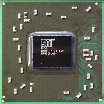
Cedar

Cedar PRO

Block Diagram
AMD's Cedar GPU uses the TeraScale 2 architecture and is made using a 40 nm production process at TSMC. With a die size of 59 mm² and a transistor count of 292 million it is a very small chip. Cedar supports DirectX 11.2 (Feature Level 11_0). For GPU compute applications, OpenCL version 1.2 can be used. It features 80 shading units, 8 texture mapping units and 4 ROPs.
Further reading:
Evergreen Series Instruction Set Architecture 
Graphics Processor
- Released
- Jan 31st, 2011
- GPU Name
- Cedar
- Mobile Variant
- Park / Robson
- Generation
- Evergreen
- Architecture
- TeraScale 2
- Foundry
- TSMC
- Process Size
- 40 nm
- Transistors
- 292 million
- Density
- 4.9M / mm²
- Die Size
- 59 mm²
- Package
- FCBGA-631
Graphics Features
- DirectX
- 11.2 (11_0)
- OpenGL
- 4.4
- OpenCL
- 1.2
- Vulkan
- N/A
- Shader Model
- 5.0
- WDDM
- 1.3
- Compute
- GFX4
- DCE
- 4.0
- UVD
- 2.3
Render Config
- Shading Units
- 80
- TMUs
- 8
- ROPs
- 4
- Compute Units
- 2
- Z-Stencil
- 4
- L1 Cache
- 8 KB per CU
- L2 Cache
- 128 KB
- Max. TDP
- 25 W
All TeraScale 2 GPUs
- AMD Barts
- AMD Blackcomb
- ATI Broadway
- AMD Broadway
- AMD Caicos
- AMD Capilano
- ATI Cedar
- AMD Cedar
- ATI Cypress
- AMD Cypress
- AMD Granville
- ATI Hemlock
- AMD Juniper
- ATI Juniper
- AMD Latte
- AMD Lexington
- AMD Loveland
- ATI Madison
- AMD Onega
- ATI Park
- AMD Park
- ATI Pinewood
- AMD Pinewood
- ATI Redwood
- AMD Redwood
- AMD Robson
- AMD Seymour
- AMD Sumo
- AMD SuperSumo
- AMD Thames
- AMD Turks
- ATI Turks
- AMD Whistler
AMD GPU Architecture History
Graphics cards using the AMD Cedar GPU
| Name | Chip | Memory | Shaders | TMUs | ROPs | GPU Clock | Memory Clock |
|---|---|---|---|---|---|---|---|
| Cedar PRO | 512 MB | 80 | 8 | 4 | 650 MHz | 500 MHz | |
| 512 MB | 80 | 8 | 4 | 650 MHz | 800 MHz | ||
| Cedar WS | 512 MB | 80 | 8 | 4 | 600 MHz | 600 MHz | |
| 512 MB | 80 | 8 | 4 | 650 MHz | 800 MHz | ||
| 1024 MB | 80 | 8 | 4 | 650 MHz | 667 MHz | ||
| Cedar PRO | 512 MB | 80 | 8 | 4 | 650 MHz | 500 MHz | |
| Cedar LE | 1024 MB | 80 | 8 | 4 | 650 MHz | 800 MHz | |
| 512 MB | 80 | 8 | 4 | 650 MHz | 500 MHz | ||
| Cedar PRO | 1024 MB | 80 | 8 | 4 | 650 MHz | 533 MHz | |
| Cedar WS | 512 MB | 80 | 8 | 4 | 600 MHz | 600 MHz |


Cedar GPU Notes
| Generation: Evergreen Mobile Variant: Park / Robson Graphics/Compute: GFX4 Display Core Engine: 4.0 Unified Video Decoder: 2.3 |
Apr 18th, 2024 03:01 EDT
change timezone
Latest GPU Drivers
New Forum Posts
- Gigabyte gpu model differences? (28)
- FINAL FANTASY XIV: Dawntrail Official Benchmark (47)
- What are you playing? (20451)
- EDP other basically constantly red while playing games (2)
- Realtek Modded Audio Driver for Windows 10/11 - Only for HDAUDIO (5675)
- AMD RX 7000 series GPU Owners' Club (1064)
- Will a RTX 4070 TI super bottleneck a Ryzen 9 7950X3D? (28)
- Identify my GPU - RX 570 8GB (or what?) (0)
- What's your latest tech purchase? (20253)
- 4K Gamers, How much VRAM do you have? (131)
Popular Reviews
- Horizon Forbidden West Performance Benchmark Review - 30 GPUs Tested
- PowerColor Radeon RX 7900 GRE Hellhound Review
- ASUS GeForce RTX 4090 Matrix Platinum Review - The RTX 4090 Ti
- Fractal Design Terra Review
- Corsair 2000D Airflow Review
- Minisforum EliteMini UM780 XTX (AMD Ryzen 7 7840HS) Review
- Creative Pebble X Plus Review
- FiiO KB3 HiFi Mechanical Keyboard Review - Integrated DAC/Amp!
- ASUS GeForce RTX 4090 STRIX OC Review
- NVIDIA GeForce RTX 4090 Founders Edition Review - Impressive Performance
Controversial News Posts
- Sony PlayStation 5 Pro Specifications Confirmed, Console Arrives Before Holidays (105)
- NVIDIA Points Intel Raptor Lake CPU Users to Get Help from Intel Amid System Instability Issues (102)
- US Government Wants Nuclear Plants to Offload AI Data Center Expansion (98)
- Windows 10 Security Updates to Cost $61 After 2025, $427 by 2028 (82)
- Developers of Outpost Infinity Siege Recommend Underclocking i9-13900K and i9-14900K for Stability on Machines with RTX 4090 (82)
- TechPowerUp Hiring: Reviewers Wanted for Motherboards, Laptops, Gaming Handhelds and Prebuilt Desktops (71)
- Intel Realizes the Only Way to Save x86 is to Democratize it, Reopens x86 IP Licensing (70)
- AMD Zen 5 Execution Engine Leaked, Features True 512-bit FPU (63)