Report an Error


AMD Exo

Exo S3 PRO

216-0867071

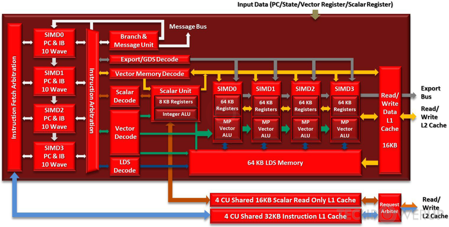
Block Diagram
CU Diagram
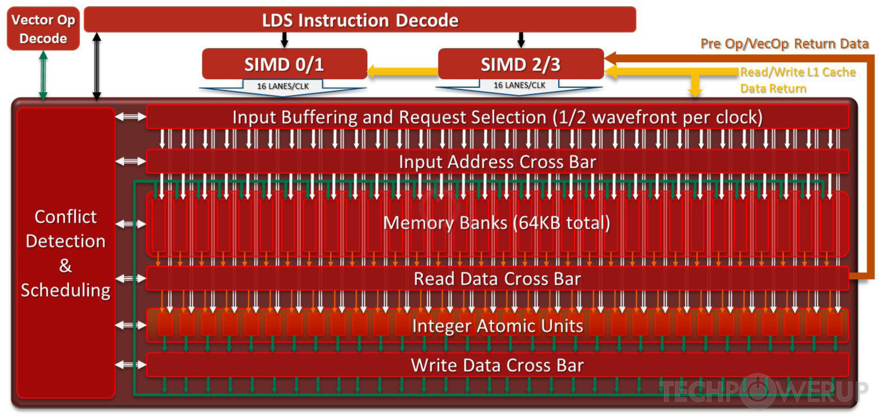
LDS Diagram
AMD's Exo GPU uses the GCN 1.0 architecture and is made using a 28 nm production process at TSMC. With a die size of 56 mm² and a transistor count of 690 million it is a very small chip. Exo supports DirectX 12 (Feature Level 11_1). For GPU compute applications, OpenCL version 2.1 (1.2) can be used. It features 320 shading units, 20 texture mapping units and 8 ROPs.
Further reading:
GCN 1.0 Architecture Whitepaper  , Sea Islands Instruction Set Architecture
Graphics Processor
- Released
- May 5th, 2015
- GPU Name
- Exo
- Desktop Variant
- Hainan
- Mobile Variant
- Sun / Jet / Banks
- Generation
- Sea Islands
- Architecture
- GCN 1.0
- Foundry
- TSMC
- Process Size
- 28 nm
- Transistors
- 690 million
- Density
- 12.3M / mm²
- Die Size
- 56 mm²
- Package
- FCBGA-631
Graphics Features
- DirectX
- 12 (11_1)
- OpenGL
- 4.6
- OpenCL
- 2.1 (1.2)
- Vulkan
- 1.2.170
- Shader Model
- 6.5 (5.1)
- WDDM
- 2.7
- Compute
- GFX6 (gfx601)
- DCE
- No Support
- UVD
- No Support
- VCE
- No Support
- CLRX
- GCN 1.0.0
Render Config
- Shading Units
- 320
- TMUs
- 20
- ROPs
- 8
- Compute Units
- 5
- ACEs
- 2
- GEs
- 1
- L1 Cache
- 16 KB per CU
- L2 Cache
- 128 KB
- Max. TDP
- 50 W
All GCN 1.0 GPUs
AMD GPU Architecture History
- 2023 CDNA 3.0
- 2022-2024 RDNA 3.0
- 2021 CDNA 2.0
- 2020 CDNA 1.0
- 2020-2023 RDNA 2.0
- 2019-2020 RDNA 1.0
- 2018-2022 GCN 5.1
- 2017-2020 GCN 5.0
- 2016-2020 GCN 4.0
- 2014-2019 GCN 3.0
- 2013-2017 GCN 2.0
- 2011-2020 GCN 1.0
- 2010-2013 TeraScale 3
- 2009-2015 TeraScale 2
- 2005-2013 TeraScale
- 2005-2007 Ultra-Threaded SE
Graphics cards using the AMD Exo GPU
| Name | Chip | Memory | Shaders | TMUs | ROPs | Base Clock | Boost Clock | Memory Clock |
|---|---|---|---|---|---|---|---|---|
| Exo S3 PRO | 2 GB | 320 | 20 | 8 | 955 MHz | 1030 MHz | 900 MHz | |
| Exo S3 PRO | 2 GB | 320 | 20 | 8 | 1030 MHz | 900 MHz | ||
| Exo S3 UL | 2 GB | 320 | 20 | 8 | 830 MHz | 855 MHz | 900 MHz | |
| Exo S3 PRO | 2 GB | 320 | 20 | 8 | 1030 MHz | 900 MHz | ||
| 2 GB | 320 | 20 | 8 | 1070 MHz | 900 MHz | |||
| 2 GB | 320 | 20 | 8 | 1030 MHz | 900 MHz |

Exo GPU Notes
| Generation: Sea Islands Desktop Variant: Hainan Mobile Variant: Sun / Jet / Banks Graphics/Compute: GFX6 (gfx601) Display Core Engine: No Support Unified Video Decoder: No Support Video Compression Engine: No Support CLRX: GCN 1.0 |
Apr 18th, 2024 09:07 EDT
change timezone
Latest GPU Drivers
New Forum Posts
- Last game you purchased? (237)
- Chinese Salvaged X99 Boards? (0)
- What phone you use as your daily driver? And, a discussion of them. (1439)
- What are you playing? (20455)
- Need help to fix my Micro-Stuttering problem (35)
- Crystaldiskinfo 8% bad state (6)
- How Much Storage Is Enough To You? (231)
- What's your latest tech purchase? (20256)
- [Official] Meta Quest 3 (44)
- Realtek Modded Audio Driver for Windows 10/11 - Only for HDAUDIO (5678)
Popular Reviews
- Horizon Forbidden West Performance Benchmark Review - 30 GPUs Tested
- PowerColor Radeon RX 7900 GRE Hellhound Review
- Fractal Design Terra Review
- Corsair 2000D Airflow Review
- Minisforum EliteMini UM780 XTX (AMD Ryzen 7 7840HS) Review
- Creative Pebble X Plus Review
- FiiO KB3 HiFi Mechanical Keyboard Review - Integrated DAC/Amp!
- ASUS GeForce RTX 4090 STRIX OC Review
- NVIDIA GeForce RTX 4090 Founders Edition Review - Impressive Performance
- ASUS GeForce RTX 4090 Matrix Platinum Review - The RTX 4090 Ti
Controversial News Posts
- Sony PlayStation 5 Pro Specifications Confirmed, Console Arrives Before Holidays (106)
- NVIDIA Points Intel Raptor Lake CPU Users to Get Help from Intel Amid System Instability Issues (102)
- US Government Wants Nuclear Plants to Offload AI Data Center Expansion (98)
- Windows 10 Security Updates to Cost $61 After 2025, $427 by 2028 (82)
- Developers of Outpost Infinity Siege Recommend Underclocking i9-13900K and i9-14900K for Stability on Machines with RTX 4090 (82)
- TechPowerUp Hiring: Reviewers Wanted for Motherboards, Laptops, Gaming Handhelds and Prebuilt Desktops (71)
- Intel Realizes the Only Way to Save x86 is to Democratize it, Reopens x86 IP Licensing (70)
- AMD Zen 5 Execution Engine Leaked, Features True 512-bit FPU (63)