Report an Error


AMD Grenada

Grenada

Fritzchens Fritz
Die Shot
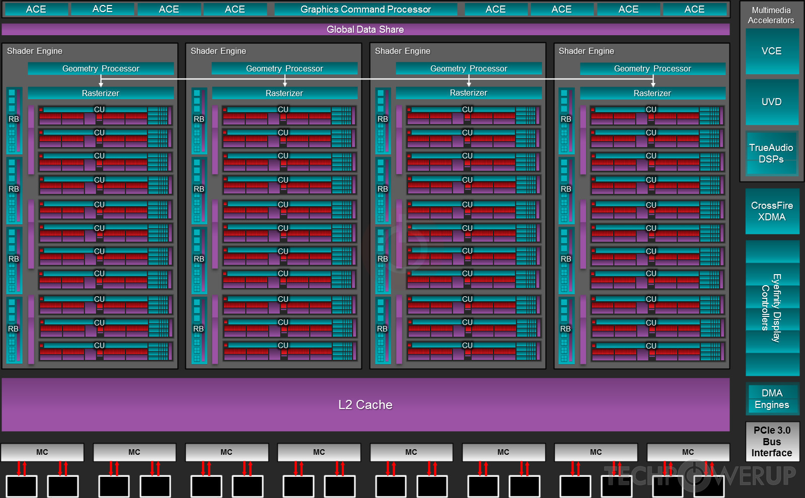
Block Diagram

SE Diagram
AMD's Grenada GPU uses the GCN 2.0 architecture and is made using a 28 nm production process at TSMC. With a die size of 438 mm² and a transistor count of 6,200 million it is a very big chip. Grenada supports DirectX 12 (Feature Level 12_0). For GPU compute applications, OpenCL version 2.1 can be used. It features 2816 shading units, 176 texture mapping units and 64 ROPs.
Graphics Processor
- Released
- Jun 18th, 2015
- GPU Name
- Grenada
- Desktop Variant
- Hawaii / Vesuvius
- Generation
- Volcanic Islands
- Architecture
- GCN 2.0
- Foundry
- TSMC
- Process Size
- 28 nm
- Transistors
- 6,200 million
- Density
- 14.2M / mm²
- Die Size
- 438 mm²
Graphics Features
- DirectX
- 12 (12_0)
- OpenGL
- 4.6
- OpenCL
- 2.1
- Vulkan
- 1.2.170
- Shader Model
- 6.5
- WDDM
- 2.7
- Compute
- GFX7 (gfx702)
- DCE
- 8.5
- UVD
- 4.2
- VCE
- 2.0
- SDMA
- 1.0.0
- CLRX
- GCN 1.1.0
Render Config
- Shading Units
- 2816
- TMUs
- 176
- ROPs
- 64
- Compute Units
- 44
- Z-Stencil
- 256
- ACEs
- 8
- GEs
- 4
- L1 Cache
- 16 KB per CU
- L2 Cache
- 1024 KB
- Max. TDP
- 580 W
All GCN 2.0 GPUs
AMD GPU Architecture History
- 2023 CDNA 3.0
- 2022-2024 RDNA 3.0
- 2021 CDNA 2.0
- 2020 CDNA 1.0
- 2020-2023 RDNA 2.0
- 2019-2020 RDNA 1.0
- 2018-2022 GCN 5.1
- 2017-2020 GCN 5.0
- 2016-2020 GCN 4.0
- 2014-2019 GCN 3.0
- 2013-2017 GCN 2.0
- 2011-2020 GCN 1.0
- 2010-2013 TeraScale 3
- 2009-2015 TeraScale 2
- 2005-2013 TeraScale
- 2005-2007 Ultra-Threaded SE
Graphics cards using the AMD Grenada GPU
| Name | Chip | Memory | Shaders | TMUs | ROPs | GPU Clock | Memory Clock |
|---|---|---|---|---|---|---|---|
| Grenada XT | 8 GB | 2816 | 176 | 64 | 1050 MHz | 1500 MHz | |
| Grenada PRO | 8 GB | 2560 | 160 | 64 | 1000 MHz | 1500 MHz | |
| Grenada PRO | 8 GB | 2560 | 160 | 64 | 1000 MHz | 1350 MHz |


Grenada GPU Notes
| Generation: Volcanic Islands Desktop Variant: Hawaii / Vesuvius Graphics/Compute: GFX7 (gfx702) Display Core Engine: 8.5 Unified Video Decoder: 4.2 Video Compression Engine: 2.0 System DMA: 1.0.0 CLRX: GCN 1.1.0 |
Apr 23rd, 2024 06:27 EDT
change timezone
Latest GPU Drivers
New Forum Posts
- My computer setup - Request for opinions (2)
- Alphacool CORE 1 CPU block - bulging with danger of splitting? (3)
- Share your AIDA 64 cache and memory benchmark here (2909)
- Is there a technical reason that Windows 11 doesn't have built into it battery charge limitation? (28)
- What are you playing? (20520)
- The best *budget* ATX PC case on the market? (21)
- Red Dead Redemption using emu (3)
- What can be changed in a VBIOS file? (PCI vendor etc) (8)
- The TPU UK Clubhouse (24765)
- TPU's Nostalgic Hardware Club (18460)
Popular Reviews
- Horizon Forbidden West Performance Benchmark Review - 30 GPUs Tested
- Fractal Design Terra Review
- Corsair 2000D Airflow Review
- Thermalright Phantom Spirit 120 EVO Review
- Minisforum EliteMini UM780 XTX (AMD Ryzen 7 7840HS) Review
- ASUS GeForce RTX 4090 STRIX OC Review
- NVIDIA GeForce RTX 4090 Founders Edition Review - Impressive Performance
- ASUS GeForce RTX 4090 Matrix Platinum Review - The RTX 4090 Ti
- Creative Pebble X Plus Review
- MSI GeForce RTX 4090 Gaming X Trio Review
Controversial News Posts
- Sony PlayStation 5 Pro Specifications Confirmed, Console Arrives Before Holidays (116)
- NVIDIA Points Intel Raptor Lake CPU Users to Get Help from Intel Amid System Instability Issues (105)
- AMD "Strix Halo" Zen 5 Mobile Processor Pictured: Chiplet-based, Uses 256-bit LPDDR5X (101)
- US Government Wants Nuclear Plants to Offload AI Data Center Expansion (98)
- Windows 10 Security Updates to Cost $61 After 2025, $427 by 2028 (84)
- Developers of Outpost Infinity Siege Recommend Underclocking i9-13900K and i9-14900K for Stability on Machines with RTX 4090 (82)
- TechPowerUp Hiring: Reviewers Wanted for Motherboards, Laptops, Gaming Handhelds and Prebuilt Desktops (74)
- Intel Realizes the Only Way to Save x86 is to Democratize it, Reopens x86 IP Licensing (70)