Report an Error


AMD Heathrow

Heathrow

Block Diagram

CU Diagram
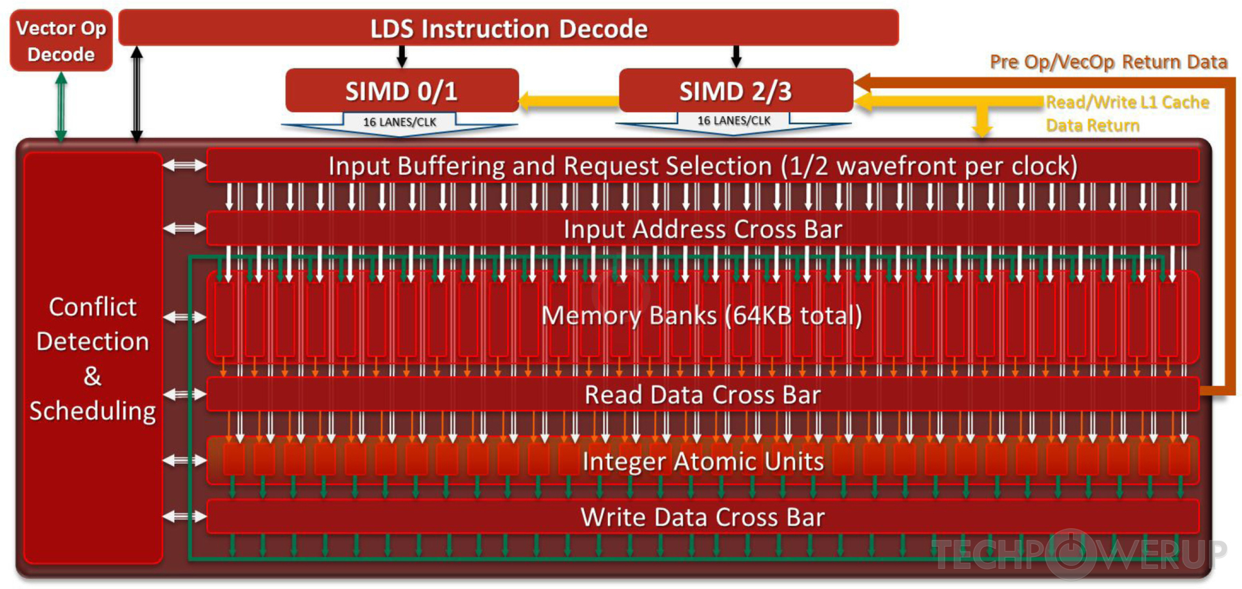
LDS Diagram
AMD's Heathrow GPU uses the GCN 1.0 architecture and is made using a 28 nm production process at TSMC. With a die size of 123 mm² and a transistor count of 1,500 million it is a small chip. Heathrow supports DirectX 12 (Feature Level 11_1). For GPU compute applications, OpenCL version 2.1 (1.2) can be used. It features 640 shading units, 40 texture mapping units and 16 ROPs.
Further reading:
GCN 1.0 Architecture Whitepaper  , Southern Islands Instruction Set Architecture
Graphics Processor
- Released
- Apr 24th, 2012
- GPU Name
- Heathrow
- Desktop Variant
- Cape Verde
- Mobile Variant
- Chelsea
- Mobile Variant 2
- Venus / Tropo
- Generation
- Southern Islands
- Architecture
- GCN 1.0
- Foundry
- TSMC
- Process Size
- 28 nm
- Transistors
- 1,500 million
- Density
- 12.2M / mm²
- Die Size
- 123 mm²
- Package
- FCBGA-962
Graphics Features
- DirectX
- 12 (11_1)
- OpenGL
- 4.6
- OpenCL
- 2.1 (1.2)
- Vulkan
- 1.2.170
- Shader Model
- 6.5 (5.1)
- WDDM
- 2.7
- Compute
- GFX6 (gfx601)
- DCE
- 6.0
- UVD
- 4.0
- VCE
- 1.0
- CLRX
- GCN 1.0.0
Render Config
- Shading Units
- 640
- TMUs
- 40
- ROPs
- 16
- Compute Units
- 10
- Z-Stencil
- 64
- ACEs
- 2
- GEs
- 1
- L1 Cache
- 16 KB per CU
- L2 Cache
- 256 KB
- Max. TDP
- 45 W
All GCN 1.0 GPUs
AMD GPU Architecture History
- 2023 CDNA 3.0
- 2022-2024 RDNA 3.0
- 2021 CDNA 2.0
- 2020 CDNA 1.0
- 2020-2023 RDNA 2.0
- 2019-2020 RDNA 1.0
- 2018-2022 GCN 5.1
- 2017-2020 GCN 5.0
- 2016-2020 GCN 4.0
- 2014-2019 GCN 3.0
- 2013-2017 GCN 2.0
- 2011-2020 GCN 1.0
- 2010-2013 TeraScale 3
- 2009-2015 TeraScale 2
- 2005-2013 TeraScale
- 2005-2007 Ultra-Threaded SE
Graphics cards using the AMD Heathrow GPU
| Name | Chip | Memory | Shaders | TMUs | ROPs | GPU Clock | Memory Clock |
|---|---|---|---|---|---|---|---|
| Heathrow PRO | 2 GB | 640 | 40 | 16 | 675 MHz | 1000 MHz | |
| Heathrow XT | 2 GB | 640 | 40 | 16 | 800 MHz | 1000 MHz | |
| Heathrow XT GL | 2 GB | 640 | 40 | 16 | 800 MHz | 1000 MHz |


Heathrow GPU Notes
| Generation: Southern Islands Desktop Variant: Cape Verde Mobile Variant: Chelsea / Venus / Tropo Graphics/Compute: GFX6 (gfx601) Display Core Engine: 6.0 Unified Video Decoder: 4.0 Video Compression Engine: 1.0 CLRX: GCN 1.0 |
Apr 25th, 2024 09:22 EDT
change timezone
Latest GPU Drivers
New Forum Posts
- RTX 4070 vs RTX 4070 Ti power scaling (5)
- i7-12800HX Overheating Issues (2)
- (Anti) SFF fun house (354)
- What's your latest tech purchase? (20339)
- Intel ARC Firmware Compilation Matrix (22)
- Alphacool CORE 1 CPU block - bulging with danger of splitting? (6)
- Bizarre Throttlestop issue (6)
- Core i5-6300U (17)
- Last game you purchased? (255)
- Share your AIDA 64 cache and memory benchmark here (2916)
Popular Reviews
- Fractal Design Terra Review
- Thermalright Phantom Spirit 120 EVO Review
- Corsair 2000D Airflow Review
- Minisforum EliteMini UM780 XTX (AMD Ryzen 7 7840HS) Review
- ASUS GeForce RTX 4090 STRIX OC Review
- NVIDIA GeForce RTX 4090 Founders Edition Review - Impressive Performance
- ASUS GeForce RTX 4090 Matrix Platinum Review - The RTX 4090 Ti
- MSI GeForce RTX 4090 Suprim X Review
- MSI GeForce RTX 4090 Gaming X Trio Review
- Gigabyte GeForce RTX 4090 Gaming OC Review
Controversial News Posts
- Sony PlayStation 5 Pro Specifications Confirmed, Console Arrives Before Holidays (116)
- NVIDIA Points Intel Raptor Lake CPU Users to Get Help from Intel Amid System Instability Issues (106)
- AMD "Strix Halo" Zen 5 Mobile Processor Pictured: Chiplet-based, Uses 256-bit LPDDR5X (101)
- US Government Wants Nuclear Plants to Offload AI Data Center Expansion (98)
- Windows 11 Now Officially Adware as Microsoft Embeds Ads in the Start Menu (88)
- Developers of Outpost Infinity Siege Recommend Underclocking i9-13900K and i9-14900K for Stability on Machines with RTX 4090 (85)
- Windows 10 Security Updates to Cost $61 After 2025, $427 by 2028 (84)
- AMD's RDNA 4 GPUs Could Stick with 18 Gbps GDDR6 Memory (81)