Report an Error


AMD Lexington
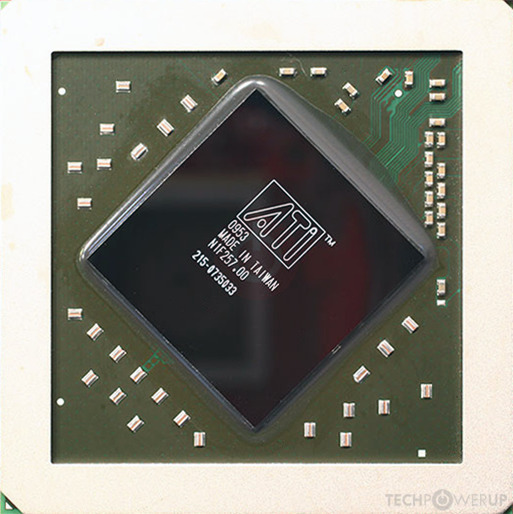
Lexington
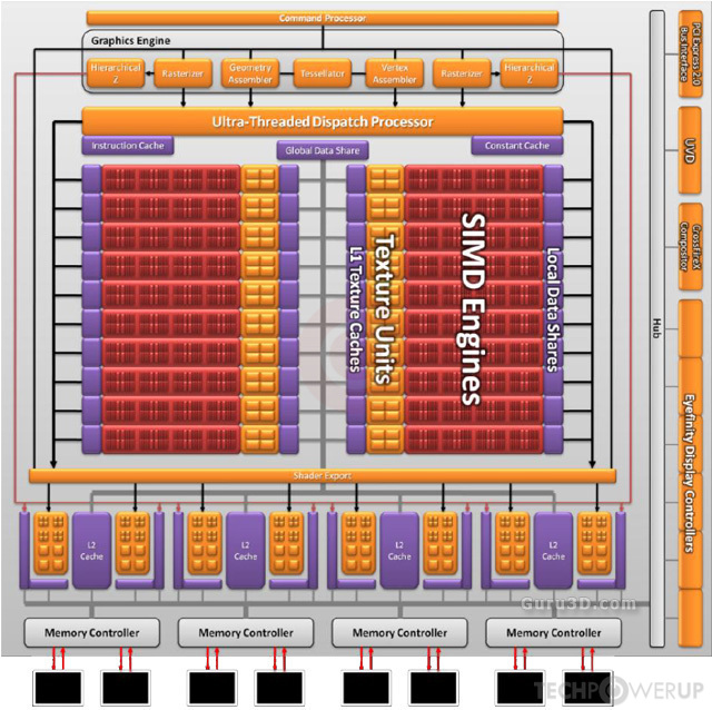
Block Diagram

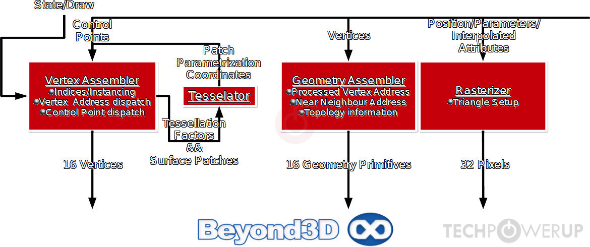
Block Diagram 2
Setup
AMD's Lexington GPU uses the TeraScale 2 architecture and is made using a 40 nm production process at TSMC. With a die size of 334 mm² and a transistor count of 2,154 million it is a large chip. Lexington supports DirectX 11.2 (Feature Level 11_0). For GPU compute applications, OpenCL version 1.2 can be used. It features 400 shading units, 20 texture mapping units and 8 ROPs.
Further reading:
Evergreen Series Instruction Set Architecture 
Graphics Processor
- Released
- Nov 26th, 2010
- GPU Name
- Lexington
- Desktop Variant
- Cypress / Hemlock
- Generation
- Evergreen
- Architecture
- TeraScale 2
- Foundry
- TSMC
- Process Size
- 40 nm
- Transistors
- 2,154 million
- Density
- 6.4M / mm²
- Die Size
- 334 mm²
Graphics Features
- DirectX
- 11.2 (11_0)
- OpenGL
- 4.4
- OpenCL
- 1.2
- Vulkan
- N/A
- Shader Model
- 5.0
- WDDM
- 1.3
- Compute
- GFX4
- DCE
- 4.0
- UVD
- 2.3
Render Config
- Shading Units
- 400
- TMUs
- 20
- ROPs
- 8
- Compute Units
- 5
- Z-Stencil
- 40
- L1 Cache
- 8 KB per CU
- L2 Cache
- 256 KB
- Max. TDP
- 26 W
All TeraScale 2 GPUs
- AMD Barts
- AMD Blackcomb
- ATI Broadway
- AMD Broadway
- AMD Caicos
- AMD Capilano
- ATI Cedar
- AMD Cedar
- ATI Cypress
- AMD Cypress
- AMD Granville
- ATI Hemlock
- AMD Juniper
- ATI Juniper
- AMD Latte
- AMD Lexington
- AMD Loveland
- ATI Madison
- AMD Onega
- ATI Park
- AMD Park
- ATI Pinewood
- AMD Pinewood
- ATI Redwood
- AMD Redwood
- AMD Robson
- AMD Seymour
- AMD Sumo
- AMD SuperSumo
- AMD Thames
- AMD Turks
- ATI Turks
- AMD Whistler
AMD GPU Architecture History
Graphics cards using the AMD Lexington GPU
| Name | Chip | Memory | Shaders | TMUs | ROPs | GPU Clock | Memory Clock |
|---|---|---|---|---|---|---|---|
| 1024 MB | 400 | 20 | 8 | 650 MHz | 900 MHz |
Lexington GPU Notes
| Generation: Evergreen Desktop Variant: Cypress / Hemlock Graphics/Compute: GFX4 Display Core Engine: 4.0 Unified Video Decoder: 2.3 |
Apr 25th, 2024 16:44 EDT
change timezone
Latest GPU Drivers
New Forum Posts
- What software are you using to monitor CPU temps during gaming session? (15)
- ROG Strix LC III 360 ARG AIO What should the pump speed be? (4)
- Ghetto Mods (4322)
- Legion Pro 7i, i9-13900HX. PL2 limit reason in log file (0)
- im new to throttelstop and i think i messed it up by copying others any hints would be very much aprreciated (2)
- Alphacool CORE 1 CPU block - bulging with danger of splitting? (15)
- What are you playing? (20528)
- What phone you use as your daily driver? And, a discussion of them. (1480)
- Black screen after muting (4)
- Micron f-die overclock issues (0)
Popular Reviews
- Fractal Design Terra Review
- Thermalright Phantom Spirit 120 EVO Review
- Corsair 2000D Airflow Review
- Minisforum EliteMini UM780 XTX (AMD Ryzen 7 7840HS) Review
- ASUS GeForce RTX 4090 STRIX OC Review
- NVIDIA GeForce RTX 4090 Founders Edition Review - Impressive Performance
- ASUS GeForce RTX 4090 Matrix Platinum Review - The RTX 4090 Ti
- MSI GeForce RTX 4090 Suprim X Review
- MSI GeForce RTX 4090 Gaming X Trio Review
- Gigabyte GeForce RTX 4090 Gaming OC Review
Controversial News Posts
- Sony PlayStation 5 Pro Specifications Confirmed, Console Arrives Before Holidays (116)
- NVIDIA Points Intel Raptor Lake CPU Users to Get Help from Intel Amid System Instability Issues (106)
- Windows 11 Now Officially Adware as Microsoft Embeds Ads in the Start Menu (104)
- AMD "Strix Halo" Zen 5 Mobile Processor Pictured: Chiplet-based, Uses 256-bit LPDDR5X (101)
- US Government Wants Nuclear Plants to Offload AI Data Center Expansion (98)
- AMD's RDNA 4 GPUs Could Stick with 18 Gbps GDDR6 Memory (86)
- Developers of Outpost Infinity Siege Recommend Underclocking i9-13900K and i9-14900K for Stability on Machines with RTX 4090 (85)
- Windows 10 Security Updates to Cost $61 After 2025, $427 by 2028 (84)