Report an Error


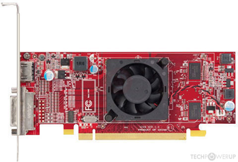
AMD Radeon HD 7450 1 GB
- Graphics Processor
- Caicos
- Cores
- 160
- TMUs
- 8
- ROPs
- 4
- Memory Size
- 1024 MB
- Memory Type
- GDDR3
- Bus Width
- 64 bit
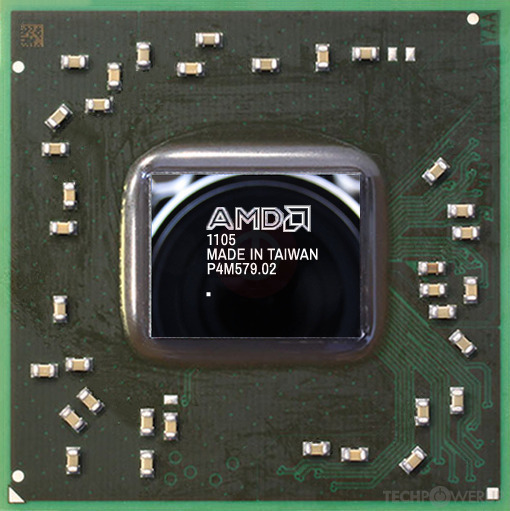
GPU
Graphics Processor
- GPU Name
- Caicos
- GPU Variant
- Caimour
- Architecture
- TeraScale 2
- Foundry
- TSMC
- Process Size
- 40 nm
- Transistors
- 370 million
- Density
- 5.5M / mm²
- Die Size
- 67 mm²
- Chip Package
- FCBGA-631
Graphics Card
- Release Date
- Jan 5th, 2012
- Generation
-
Southern Islands
(HD 7400)
- Predecessor
- Northern Islands
- Successor
- Sea Islands
- Production
- End-of-life
- Bus Interface
- PCIe 2.0 x16
Clock Speeds
- GPU Clock
625 MHz
750 MHz (+20%)
- Memory Clock
-
533 MHz
800 MHz (+50%)
1066 Mbps effective
1600 Mbps effective
Memory
- Memory Size
-
512 MB
1024 MB
- Memory Type
- GDDR3
- Memory Bus
- 64 bit
- Bandwidth
-
8.528 GB/s
12.80 GB/s
Render Config
- Shading Units
- 160
- TMUs
- 8
- ROPs
- 4
- Compute Units
- 2
- L1 Cache
- 8 KB (per CU)
- L2 Cache
- 128 KB
Theoretical Performance
- Pixel Rate
-
2.500 GPixel/s
3.000 GPixel/s
- Texture Rate
-
5.000 GTexel/s
6.000 GTexel/s
- FP32 (float)
-
200.0 GFLOPS
240.0 GFLOPS
Board Design
- Slot Width
- Single-slot
- TDP
- 18 W
- Suggested PSU
- 200 W
- Outputs
- 1x DVI
1x HDMI 1.3a
- Power Connectors
- None
- Board Number
- C264
Graphics Features
- DirectX
- 11.2 (11_0)
- OpenGL
- 4.4
- OpenCL
- 1.2
- Vulkan
- N/A
- Shader Model
- 5.0
Card Notes
| Rebranded HD 6450 DDR3 |
Caicos GPU Notes
| Generation: Northern Islands Mobile Variant: Seymour Graphics/Compute: GFX4 Display Core Engine: 5.0 Unified Video Decoder: 3.1 |
Other retail boards based on this design (6)
| Name | GPU Clock | Memory Clock | Other Changes |
|---|---|---|---|
|
AMD Radeon HD 7450 1 GB

|
750 MHz | 800 MHz | 1024 MB |
| 625 MHz | 800 MHz | 1024 MB | |
| 625 MHz | 800 MHz | 1024 MB, 1x DVI 1x DisplayPort | |
| 625 MHz | 800 MHz | 1024 MB | |
| 625 MHz | 500 MHz | 2 GB, 1x DVI 1x HDMI 1x VGA | |
| 625 MHz | 533 MHz | 1024 MB |


Apr 16th, 2024 15:09 EDT
change timezone
Latest GPU Drivers
New Forum Posts
- Time to update the motherboards layout! (106)
- which new soundcard or which 4.1 speakers kits ? (5)
- FINAL FANTASY XIV: Dawntrail Official Benchmark (36)
- cooling vrm on cheap motherboard for 5950x (14)
- Free Games Thread (3755)
- Samsung 870 EVO - Beware, certain batches prone to failure! (1129)
- Outer Worlds getting boring (24)
- What's your latest tech purchase? (20234)
- TPU's Nostalgic Hardware Club (18444)
- TPU's WCG/BOINC Team (34416)
Popular Reviews
- Horizon Forbidden West Performance Benchmark Review - 30 GPUs Tested
- PowerColor Radeon RX 7900 GRE Hellhound Review
- Galax GeForce RTX 4070 Super EX Review
- Fractal Design Terra Review
- ASUS GeForce RTX 4090 Matrix Platinum Review - The RTX 4090 Ti
- Corsair 2000D Airflow Review
- Minisforum EliteMini UM780 XTX (AMD Ryzen 7 7840HS) Review
- Creative Pebble X Plus Review
- FiiO KB3 HiFi Mechanical Keyboard Review - Integrated DAC/Amp!
- ASUS GeForce RTX 4090 STRIX OC Review
Controversial News Posts
- NVIDIA Points Intel Raptor Lake CPU Users to Get Help from Intel Amid System Instability Issues (102)
- US Government Wants Nuclear Plants to Offload AI Data Center Expansion (98)
- Sony PlayStation 5 Pro Specifications Confirmed, Console Arrives Before Holidays (95)
- Developers of Outpost Infinity Siege Recommend Underclocking i9-13900K and i9-14900K for Stability on Machines with RTX 4090 (82)
- Windows 10 Security Updates to Cost $61 After 2025, $427 by 2028 (79)
- TechPowerUp Hiring: Reviewers Wanted for Motherboards, Laptops, Gaming Handhelds and Prebuilt Desktops (70)
- Intel Realizes the Only Way to Save x86 is to Democratize it, Reopens x86 IP Licensing (70)
- AMD Zen 5 Execution Engine Leaked, Features True 512-bit FPU (63)