Report an Error


AMD Radeon HD 7470M
- Graphics Processor
- Seymour
- Cores
- 160
- TMUs
- 8
- ROPs
- 4
- Memory Size
- 1024 MB
- Memory Type
- GDDR5
- Bus Width
- 64 bit

GPU
Graphics Processor
- GPU Name
- Seymour
- GPU Variant
-
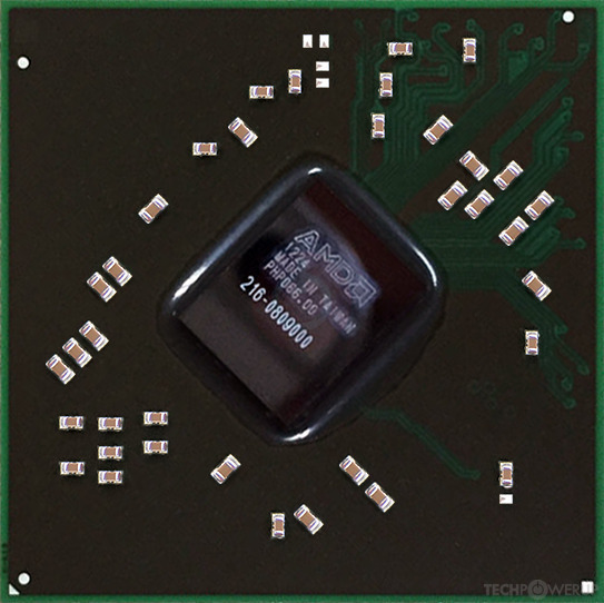
Seymour XTX M2
(216-0809000)
- Architecture
- TeraScale 2
- Foundry
- TSMC
- Process Size
- 40 nm
- Transistors
- 370 million
- Density
- 5.5M / mm²
- Die Size
- 67 mm²
- Chip Package
- FCBGA-631/962
Mobile Graphics
- Release Date
- Jan 7th, 2012
- Generation
-
London
(HD 7400M)
- Predecessor
- Vancouver
- Successor
- Solar System
- Production
- End-of-life
- Bus Interface
- PCIe 2.0 x16
Clock Speeds
- Base Clock
750 MHz
800 MHz (+7%)
- Boost Clock
- 800 MHz
- Memory Clock
-
900 MHz
800 MHz (-11%)
1800 Mbps effective
3.2 Gbps effective
Memory
- Memory Size
- 1024 MB
- Memory Type
DDR3
GDDR5
- Memory Bus
- 64 bit
- Bandwidth
-
14.40 GB/s
25.60 GB/s
Render Config
- Shading Units
- 160
- TMUs
- 8
- ROPs
- 4
- Compute Units
- 2
- L1 Cache
- 8 KB (per CU)
- L2 Cache
- 128 KB
Theoretical Performance
- Pixel Rate
- 3.200 GPixel/s
- Texture Rate
- 6.400 GTexel/s
- FP32 (float)
- 256.0 GFLOPS
Board Design
- TDP
- 25 W
- Outputs
- Portable Device Dependent
Graphics Features
- DirectX
- 11.2 (11_0)
- OpenGL
- 4.4
- OpenCL
- 1.2
- Vulkan
- N/A
- Shader Model
- 5.0
Card Notes
| Rebranded HD 6470M |
Seymour GPU Notes
| Generation: Northern Islands Desktop Variant: Caicos Graphics/Compute: GFX4 Display Core Engine: 5.0 Unified Video Decoder: 3.1 |
Other retail boards based on this design (2)
| Name | GPU Clock | Boost Clock | Memory Clock | Other Changes |
|---|---|---|---|---|
|
AMD Radeon HD 7470M

|
800 MHz | 800 MHz | 800 MHz | GDDR5 |
| 750 MHz | 800 MHz | 900 MHz | GDDR5 |

Apr 24th, 2024 20:34 EDT
change timezone
Latest GPU Drivers
New Forum Posts
- The TPU UK Clubhouse (24783)
- (Anti) SFF fun house (346)
- Cinebench crashed my PC. My Wi-Fi stopped working, and I keep getting a "Please wait" screen when I boot up my PC. (28)
- Sharing experience with MSI RTX 3070 vBIOS update to enable Resizable Bar with MB Z490 (2)
- Share your AIDA 64 cache and memory benchmark here (2915)
- Will a RTX 4070 TI super bottleneck a Ryzen 9 7950X3D? (58)
- The best *budget* ATX PC case on the market? (24)
- GTX 1070 Ti - TDP Issues - Always Power Throttling (4)
- 2022-X58/1366 PIN Motherboards NVME M.2 SSD BIOS MOD Collection (656)
- Meta Horizon OS (15)
Popular Reviews
- Fractal Design Terra Review
- Thermalright Phantom Spirit 120 EVO Review
- Corsair 2000D Airflow Review
- Minisforum EliteMini UM780 XTX (AMD Ryzen 7 7840HS) Review
- ASUS GeForce RTX 4090 STRIX OC Review
- NVIDIA GeForce RTX 4090 Founders Edition Review - Impressive Performance
- ASUS GeForce RTX 4090 Matrix Platinum Review - The RTX 4090 Ti
- MSI GeForce RTX 4090 Suprim X Review
- MSI GeForce RTX 4090 Gaming X Trio Review
- Gigabyte GeForce RTX 4090 Gaming OC Review
Controversial News Posts
- Sony PlayStation 5 Pro Specifications Confirmed, Console Arrives Before Holidays (116)
- NVIDIA Points Intel Raptor Lake CPU Users to Get Help from Intel Amid System Instability Issues (106)
- AMD "Strix Halo" Zen 5 Mobile Processor Pictured: Chiplet-based, Uses 256-bit LPDDR5X (101)
- US Government Wants Nuclear Plants to Offload AI Data Center Expansion (98)
- Windows 10 Security Updates to Cost $61 After 2025, $427 by 2028 (84)
- Developers of Outpost Infinity Siege Recommend Underclocking i9-13900K and i9-14900K for Stability on Machines with RTX 4090 (84)
- TechPowerUp Hiring: Reviewers Wanted for Motherboards, Laptops, Gaming Handhelds and Prebuilt Desktops (78)
- AMD's RDNA 4 GPUs Could Stick with 18 Gbps GDDR6 Memory (71)