Report an Error


AMD Trinidad
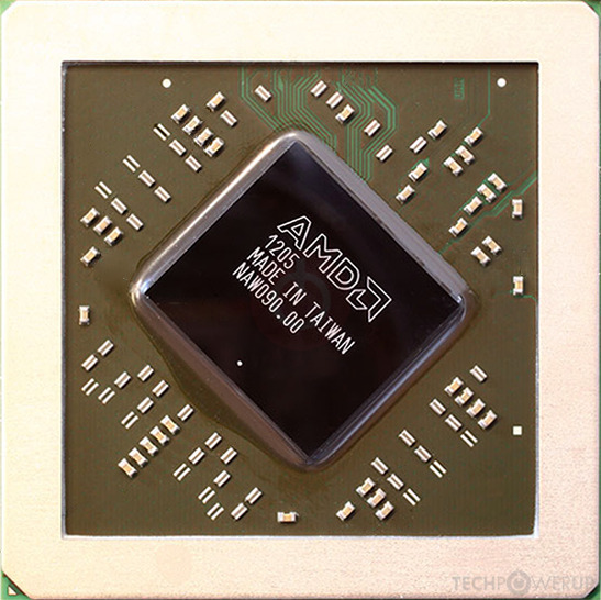
Trinidad
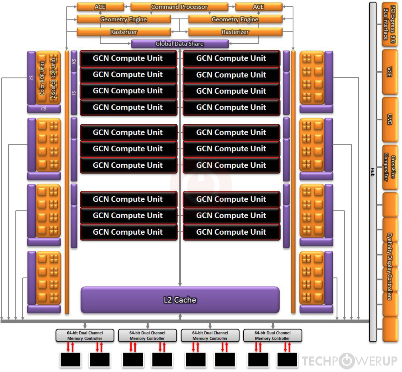
Block Diagram

CU Diagram
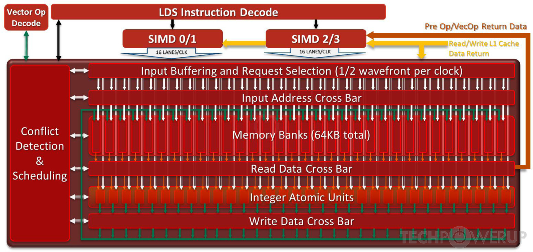
LDS Diagram
AMD's Trinidad GPU uses the GCN 1.0 architecture and is made using a 28 nm production process at TSMC. With a die size of 212 mm² and a transistor count of 2,800 million it is a medium-sized chip. Trinidad supports DirectX 12 (Feature Level 11_1). For GPU compute applications, OpenCL version 2.1 (1.2) can be used. It features 1280 shading units, 80 texture mapping units and 32 ROPs.
Further reading:
GCN 1.0 Architecture Whitepaper  , Southern Islands Instruction Set Architecture
Graphics Processor
- Released
- May 5th, 2015
- GPU Name
- Trinidad
- Desktop Variant
- Pitcairn / Curacao
- Mobile Variant
- Wimbledon/Neptune
- Generation
- Southern Islands
- Architecture
- GCN 1.0
- Foundry
- TSMC
- Process Size
- 28 nm
- Transistors
- 2,800 million
- Density
- 13.2M / mm²
- Die Size
- 212 mm²
- Package
- FCBGA-1737
Graphics Features
- DirectX
- 12 (11_1)
- OpenGL
- 4.6
- OpenCL
- 2.1 (1.2)
- Vulkan
- 1.2.170
- Shader Model
- 6.5 (5.1)
- WDDM
- 2.7
- Compute
- GFX6 (gfx601)
- DCE
- 6.0
- UVD
- 4.0
- VCE
- 1.0
- CLRX
- GCN 1.0.0
Render Config
- Shading Units
- 1280
- TMUs
- 80
- ROPs
- 32
- Compute Units
- 24
- Z-Stencil
- 128
- ACEs
- 2
- GEs
- 2
- L1 Cache
- 16 KB per CU
- L2 Cache
- 512 KB
- Max. TDP
- 180 W
All GCN 1.0 GPUs
AMD GPU Architecture History
- 2023 CDNA 3.0
- 2022-2024 RDNA 3.0
- 2021 CDNA 2.0
- 2020 CDNA 1.0
- 2020-2023 RDNA 2.0
- 2019-2020 RDNA 1.0
- 2018-2022 GCN 5.1
- 2017-2020 GCN 5.0
- 2016-2020 GCN 4.0
- 2014-2019 GCN 3.0
- 2013-2017 GCN 2.0
- 2011-2020 GCN 1.0
- 2010-2013 TeraScale 3
- 2009-2015 TeraScale 2
- 2005-2013 TeraScale
- 2005-2007 Ultra-Threaded SE
Graphics cards using the AMD Trinidad GPU
| Name | Chip | Memory | Shaders | TMUs | ROPs | Base Clock | Boost Clock | Memory Clock |
|---|---|---|---|---|---|---|---|---|
| Trinidad PRO | 2 GB | 1024 | 64 | 32 | 925 MHz | 975 MHz | 1400 MHz | |
| Trinidad PRO | 2 GB | 1280 | 80 | 32 | 925 MHz | 975 MHz | 1400 MHz | |
| Trinidad XT | 2 GB | 1280 | 80 | 32 | 980 MHz | 1030 MHz | 1400 MHz | |
| Trinidad PRO | 2 GB | 1024 | 64 | 32 | 925 MHz | 975 MHz | 1400 MHz |


Trinidad GPU Notes
| Generation: Southern Islands Desktop Variant: Pitcairn / Curacao Mobile Variant: Wimbledon / Neptune Graphics/Compute: GFX6 (gfx601) Display Core Engine: 6.0 Unified Video Decoder: 4.0 Video Compression Engine: 1.0 CLRX: GCN 1.0 |
Apr 25th, 2024 00:29 EDT
change timezone
Latest GPU Drivers
New Forum Posts
- What's your latest tech purchase? (20337)
- The Official Linux/Unix Desktop Screenshots Megathread (694)
- XFX RX470 8GB no video and error 43 (27)
- (Anti) SFF fun house (348)
- Cinebench crashed my PC. My Wi-Fi stopped working, and I keep getting a "Please wait" screen when I boot up my PC. (31)
- im new to throttelstop and i think i messed it up by copying others any hints would be very much aprreciated (1)
- Aida64 cache mem OC (7)
- I am getting artifacting when I change Windows security settings. Is my GPU failing, or is this just a Windows issue? (10)
- Is there a technical reason that Windows 11 doesn't have built into it battery charge limitation? (42)
- The TPU UK Clubhouse (24783)
Popular Reviews
- Fractal Design Terra Review
- Thermalright Phantom Spirit 120 EVO Review
- Corsair 2000D Airflow Review
- Minisforum EliteMini UM780 XTX (AMD Ryzen 7 7840HS) Review
- ASUS GeForce RTX 4090 STRIX OC Review
- NVIDIA GeForce RTX 4090 Founders Edition Review - Impressive Performance
- ASUS GeForce RTX 4090 Matrix Platinum Review - The RTX 4090 Ti
- MSI GeForce RTX 4090 Suprim X Review
- MSI GeForce RTX 4090 Gaming X Trio Review
- Gigabyte GeForce RTX 4090 Gaming OC Review
Controversial News Posts
- Sony PlayStation 5 Pro Specifications Confirmed, Console Arrives Before Holidays (116)
- NVIDIA Points Intel Raptor Lake CPU Users to Get Help from Intel Amid System Instability Issues (106)
- AMD "Strix Halo" Zen 5 Mobile Processor Pictured: Chiplet-based, Uses 256-bit LPDDR5X (101)
- US Government Wants Nuclear Plants to Offload AI Data Center Expansion (98)
- Windows 10 Security Updates to Cost $61 After 2025, $427 by 2028 (84)
- Developers of Outpost Infinity Siege Recommend Underclocking i9-13900K and i9-14900K for Stability on Machines with RTX 4090 (84)
- TechPowerUp Hiring: Reviewers Wanted for Motherboards, Laptops, Gaming Handhelds and Prebuilt Desktops (78)
- AMD's RDNA 4 GPUs Could Stick with 18 Gbps GDDR6 Memory (73)