Report an Error


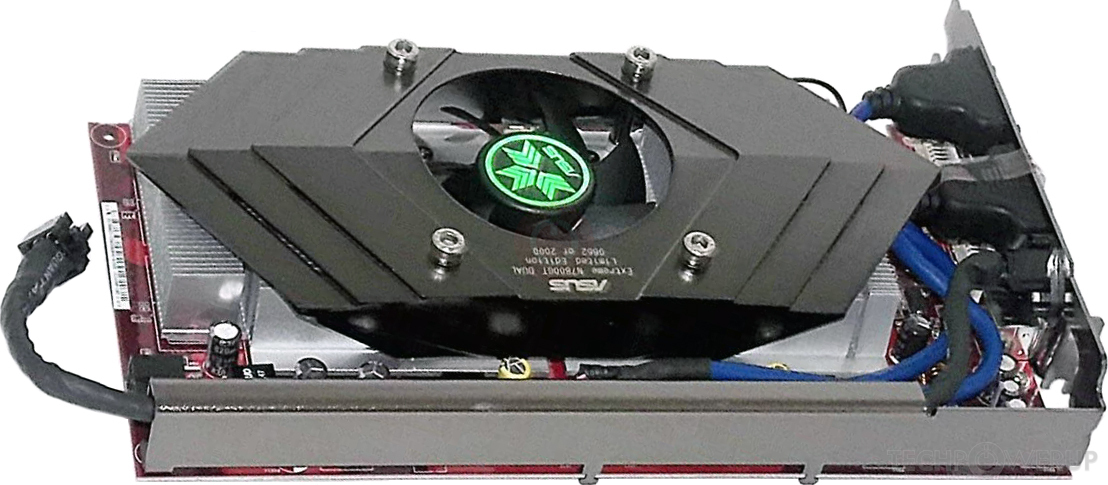
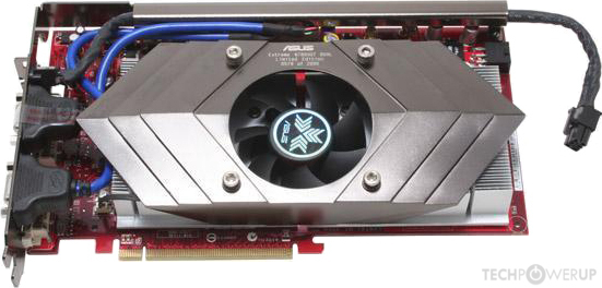
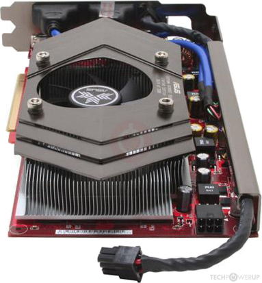
ASUS 7800 GT Dual
- EN7800GT-DUAL/2DHTV/512M
- Graphics Processor
- G70 x2
- Pixel Shaders
- 20 x2
- Vertex Shaders
- 7 x2
- TMUs
- 20 x2
- ROPs
- 16 x2
- Memory Size
- 256 MB x2
- Memory Type
- GDDR3
- Bus Width
- 256 bit x2


GPU

I/O
Top
Bottom
Rear

Back
Graphics Processor
Graphics Card
- Release Date
Aug 11th, 2005
Dec 14th, 2005
- Generation
-
GeForce 7 PCIe
(7800)
- Predecessor
- GeForce 6 PCIe
- Successor
- GeForce 8
- Production
- End-of-life
- Bus Interface
- PCIe 1.0 x16
Clock Speeds
- GPU Clock
400 MHz
430 MHz (+8%)
- Memory Clock
-
500 MHz
600 MHz (+20%)
1000 Mbps effective
1200 Mbps effective
Memory
- Memory Size
- 256 MB
- Memory Type
- GDDR3
- Memory Bus
- 256 bit
- Bandwidth
-
32.00 GB/s
38.40 GB/s
Render Config
- Pixel Shaders
- 20
- Vertex Shaders
- 7
- TMUs
- 20
- ROPs
- 16
Theoretical Performance
- Pixel Rate
-
6.400 GPixel/s
6.880 GPixel/s
- Vertex Rate
-
700.0 MVertices/s
752.5 MVertices/s
- Texture Rate
-
8.000 GTexel/s
8.600 GTexel/s
Board Design
- Slot Width
- Dual-slot
- TDP
- 120 W
- Suggested PSU
- 300 W
- Outputs
- 2x DVI
2x VGA
1x S-Video
- Power Connectors
- 1x 6-pin
- Board Number
- P317 SKU 0
Graphics Features
- DirectX
- 9.0c (9_3)
- OpenGL
- 2.1
- OpenCL
- N/A
- Vulkan
- N/A
- Shader Model
- 3.0
G70 GPU Notes
| PureVideo HD: VP1 VDPAU: No Support |
Other retail boards based on this design (1)
| Name | GPU Clock | Memory Clock | Other Changes |
|---|---|---|---|
|
ASUS 7800 GT Dual

|
430 MHz | 600 MHz |
Apr 25th, 2024 01:45 EDT
change timezone
Latest GPU Drivers
New Forum Posts
- The TPU UK Clubhouse (24784)
- (Anti) SFF fun house (349)
- Github comments used to push malware via Microsoft repo urls (1)
- What's your latest tech purchase? (20337)
- The Official Linux/Unix Desktop Screenshots Megathread (694)
- XFX RX470 8GB no video and error 43 (27)
- Cinebench crashed my PC. My Wi-Fi stopped working, and I keep getting a "Please wait" screen when I boot up my PC. (31)
- im new to throttelstop and i think i messed it up by copying others any hints would be very much aprreciated (1)
- Aida64 cache mem OC (7)
- I am getting artifacting when I change Windows security settings. Is my GPU failing, or is this just a Windows issue? (10)
Popular Reviews
- Fractal Design Terra Review
- Thermalright Phantom Spirit 120 EVO Review
- Corsair 2000D Airflow Review
- Minisforum EliteMini UM780 XTX (AMD Ryzen 7 7840HS) Review
- ASUS GeForce RTX 4090 STRIX OC Review
- NVIDIA GeForce RTX 4090 Founders Edition Review - Impressive Performance
- ASUS GeForce RTX 4090 Matrix Platinum Review - The RTX 4090 Ti
- MSI GeForce RTX 4090 Suprim X Review
- MSI GeForce RTX 4090 Gaming X Trio Review
- Gigabyte GeForce RTX 4090 Gaming OC Review
Controversial News Posts
- Sony PlayStation 5 Pro Specifications Confirmed, Console Arrives Before Holidays (116)
- NVIDIA Points Intel Raptor Lake CPU Users to Get Help from Intel Amid System Instability Issues (106)
- AMD "Strix Halo" Zen 5 Mobile Processor Pictured: Chiplet-based, Uses 256-bit LPDDR5X (101)
- US Government Wants Nuclear Plants to Offload AI Data Center Expansion (98)
- Windows 10 Security Updates to Cost $61 After 2025, $427 by 2028 (84)
- Developers of Outpost Infinity Siege Recommend Underclocking i9-13900K and i9-14900K for Stability on Machines with RTX 4090 (84)
- TechPowerUp Hiring: Reviewers Wanted for Motherboards, Laptops, Gaming Handhelds and Prebuilt Desktops (78)
- AMD's RDNA 4 GPUs Could Stick with 18 Gbps GDDR6 Memory (74)