Report an Error


ASUS 8800 GTS TOP
- EN8800GTS-TOP/HTDP/512M
- Graphics Processor
- G92
- Cores
- 128
- TMUs
- 64
- ROPs
- 16
- Memory Size
- 512 MB
- Memory Type
- GDDR3
- Bus Width
- 256 bit

GPU
Graphics Processor
Graphics Card
- Release Date
- Dec 11th, 2007
- Generation
-
GeForce 8
(8800)
- Predecessor
- GeForce 7 PCIe
- Successor
- GeForce 9
- Production
- End-of-life
- Bus Interface
- PCIe 2.0 x16
Clock Speeds
- GPU Clock
650 MHz
740 MHz (+14%)
- Shader Clock
1625 MHz
1800 MHz (+11%)
- Memory Clock
-
820 MHz
1035 MHz (+26%)
1640 Mbps effective
2.1 Gbps effective
Memory
- Memory Size
- 512 MB
- Memory Type
- GDDR3
- Memory Bus
- 256 bit
- Bandwidth
-
52.48 GB/s
66.24 GB/s
Render Config
- Shading Units
- 128
- TMUs
- 64
- ROPs
- 16
- SM Count
- 16
- L2 Cache
- 64 KB
Theoretical Performance
- Pixel Rate
-
10.40 GPixel/s
11.84 GPixel/s
- Texture Rate
-
41.60 GTexel/s
47.36 GTexel/s
- FP32 (float)
-
416.0 GFLOPS
460.8 GFLOPS
Board Design
- Slot Width
- Dual-slot
- Length
254 mm
267 mm
10 inches
10.5 inches
- TDP
- 135 W
- Suggested PSU
- 300 W
- Outputs
- 2x DVI
1x S-Video
- Power Connectors
- 1x 6-pin
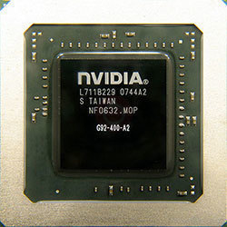
- Board Number
- P393 SKU 0
Graphics Features
- DirectX
- 11.1 (10_0)
- OpenGL
- 3.3
- OpenCL
- 1.1
- Vulkan
- N/A
- CUDA
- 1.1
- Shader Model
- 4.0
G92 GPU Notes
| PureVideo HD: VP2 VDPAU: Feature Set A |
Other retail boards based on this design (3)
| Name | GPU Clock | Memory Clock | Other Changes |
|---|---|---|---|
|
ASUS 8800 GTS TOP

|
740 MHz | 1035 MHz | 267 mm/10.5 inches |
| 730 MHz | 1050 MHz | 1024 MB, 229 mm/9 inches | |
| 678 MHz | 972 MHz | 229 mm/9 inches |


Apr 18th, 2024 21:44 EDT
change timezone
Latest GPU Drivers
New Forum Posts
- What's your latest tech purchase? (20274)
- Cinebench crashed my PC. My Wi-Fi stopped working, and I keep getting a "Please wait" screen when I boot up my PC. (2)
- Should the CDPR make the Fallout 5 instead? (13)
- Why is SteamOS taking so long to come to desktop for AMD users, when ChimeraOS is the same thing almost? (17)
- DDR5 RAM Speeds and the future (39)
- XFX RX560 1024 shaders 16 CU 4GB from Aliexpress (6)
- Is it possible that the atmosphere is losing less of its "shield" capabilities due to more and more jets/rockets puncturing it daily? (25)
- Do you use Linux? (228)
- FINAL FANTASY XIV: Dawntrail Official Benchmark (55)
- MSI Z790 owners - be careful, the screw can crack the chipset (5)
Popular Reviews
- Horizon Forbidden West Performance Benchmark Review - 30 GPUs Tested
- PowerColor Radeon RX 7900 GRE Hellhound Review
- Fractal Design Terra Review
- Corsair 2000D Airflow Review
- Minisforum EliteMini UM780 XTX (AMD Ryzen 7 7840HS) Review
- Thermalright Phantom Spirit 120 EVO Review
- Creative Pebble X Plus Review
- FiiO KB3 HiFi Mechanical Keyboard Review - Integrated DAC/Amp!
- ASUS GeForce RTX 4090 STRIX OC Review
- NVIDIA GeForce RTX 4090 Founders Edition Review - Impressive Performance
Controversial News Posts
- Sony PlayStation 5 Pro Specifications Confirmed, Console Arrives Before Holidays (109)
- NVIDIA Points Intel Raptor Lake CPU Users to Get Help from Intel Amid System Instability Issues (102)
- US Government Wants Nuclear Plants to Offload AI Data Center Expansion (98)
- Windows 10 Security Updates to Cost $61 After 2025, $427 by 2028 (82)
- Developers of Outpost Infinity Siege Recommend Underclocking i9-13900K and i9-14900K for Stability on Machines with RTX 4090 (82)
- TechPowerUp Hiring: Reviewers Wanted for Motherboards, Laptops, Gaming Handhelds and Prebuilt Desktops (71)
- Intel Realizes the Only Way to Save x86 is to Democratize it, Reopens x86 IP Licensing (70)
- AMD Zen 5 Execution Engine Leaked, Features True 512-bit FPU (63)