Report an Error


ATI M9

M9

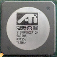
M9 9000

M9
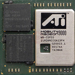
M9-CSP32
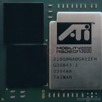
M9-CSP64GL

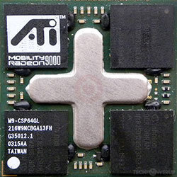
M9-CSP64
ATI's M9 GPU uses the Rage 7 architecture and is made using a 150 nm production process at TSMC. With a die size of 81 mm² and a transistor count of 36 million it is a very small chip. M9 supports DirectX 8.1. Modern GPU compute technologies are not available. It features 4 pixel shaders and 1 vertex shaders, 4 texture mapping units and 4 ROPs. Due to the lack of unified shaders you will not be able to run recent games at all (which require unified shader/DX10+ support).
Graphics Processor
- Released
- 2002
- GPU Name
- M9
- Desktop Variant
- RV280
- Codename
- Argus
- Architecture
- Rage 7
- Foundry
- TSMC
- Package
- BGA-650
- Process Size
- 150 nm
- Transistors
- 36 million
- Density
- 444.4K / mm²
- Die Size
- 81 mm²
Graphics Features
- DirectX
- 8.1
- OpenGL
- 1.4
- OpenCL
- N/A
- Vulkan
- N/A
- Pixel Shader
- 1.4
- Vertex Shader
- 1.1
- Compute
- GFX1
Render Config
- Pixel Shaders
- 4
- Vertex Shaders
- 1
- TMUs
- 4
- ROPs
- 4
All Rage 7 GPUs
ATI GPU Architecture History
Graphics cards using the ATI M9 GPU
| Name | Chip | Memory | Shaders | TMUs | ROPs | GPU Clock | Memory Clock |
|---|---|---|---|---|---|---|---|
| M9 9000 | 64 MB | 4 / 1 | 4 | 4 | 240 MHz | 200 MHz | |
| M9-CSP64GL | 64 MB | 4 / 1 | 4 | 4 | 250 MHz | 200 MHz | |
| M9-CSP32 | 32 MB | 4 / 1 | 4 | 4 | 240 MHz | 200 MHz | |
| M9-CSP64 | 64 MB | 4 / 1 | 4 | 4 | 240 MHz | 200 MHz |


M9 GPU Notes
| Desktop Variant: RV280 Codename: Argus Graphics/Compute: GFX1 Smart Shader 1.0 Smooth Vision 1.0 TruForm 1.0 FullStream Hyper Z II Video Shader Video Immersion II Programmable pixel&vertex pipelines M9 Chip Numbers: M9-CSP64GL (216W9NCBGA12FH) |
Apr 24th, 2024 06:55 EDT
change timezone
Latest GPU Drivers
New Forum Posts
- Will a RTX 4070 TI super bottleneck a Ryzen 9 7950X3D? (52)
- The TPU UK Clubhouse (24778)
- My computer setup - Request for opinions (14)
- EK seems to be having major issues (31)
- Windows 11 General Discussion (5023)
- What's your latest tech purchase? (20331)
- Share your AIDA 64 cache and memory benchmark here (2914)
- CYBERPUNK 2077 O.F. (5)
- What phone you use as your daily driver? And, a discussion of them. (1458)
- Which new games will you be buying? (309)
Popular Reviews
- Fractal Design Terra Review
- Corsair 2000D Airflow Review
- Thermalright Phantom Spirit 120 EVO Review
- Minisforum EliteMini UM780 XTX (AMD Ryzen 7 7840HS) Review
- ASUS GeForce RTX 4090 STRIX OC Review
- NVIDIA GeForce RTX 4090 Founders Edition Review - Impressive Performance
- ASUS GeForce RTX 4090 Matrix Platinum Review - The RTX 4090 Ti
- MSI GeForce RTX 4090 Suprim X Review
- MSI GeForce RTX 4090 Gaming X Trio Review
- Gigabyte GeForce RTX 4090 Gaming OC Review
Controversial News Posts
- Sony PlayStation 5 Pro Specifications Confirmed, Console Arrives Before Holidays (116)
- NVIDIA Points Intel Raptor Lake CPU Users to Get Help from Intel Amid System Instability Issues (106)
- AMD "Strix Halo" Zen 5 Mobile Processor Pictured: Chiplet-based, Uses 256-bit LPDDR5X (101)
- US Government Wants Nuclear Plants to Offload AI Data Center Expansion (98)
- Windows 10 Security Updates to Cost $61 After 2025, $427 by 2028 (84)
- Developers of Outpost Infinity Siege Recommend Underclocking i9-13900K and i9-14900K for Stability on Machines with RTX 4090 (84)
- TechPowerUp Hiring: Reviewers Wanted for Motherboards, Laptops, Gaming Handhelds and Prebuilt Desktops (77)
- Intel Realizes the Only Way to Save x86 is to Democratize it, Reopens x86 IP Licensing (70)