Report an Error


ATI RV350

RV350

RV350 LE

RV350 LX

RV350 XT
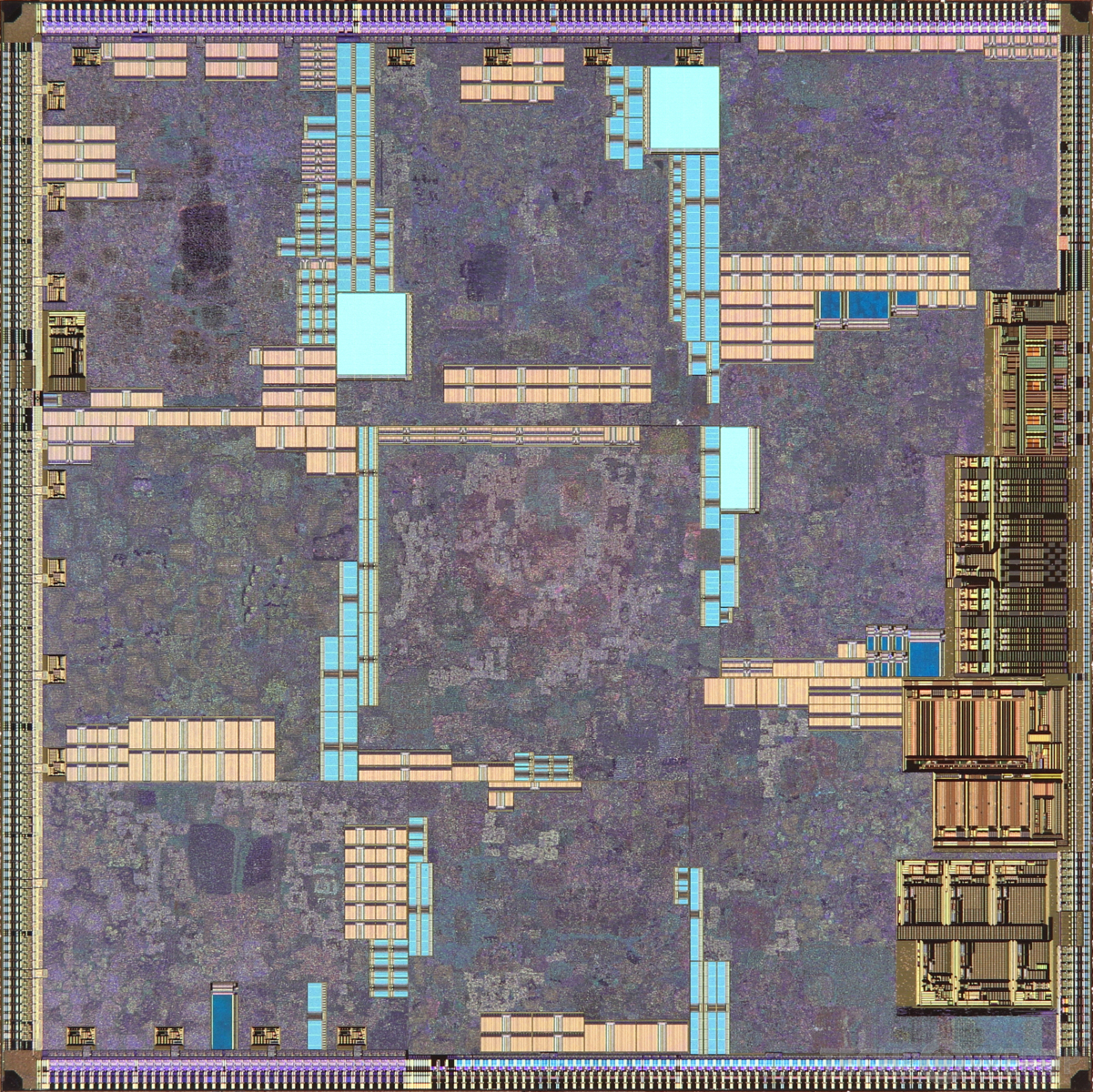
Die Shot
ATI's RV350 GPU uses the R300 architecture and is made using a 130 nm production process at TSMC. With a die size of 76 mm² and a transistor count of 60 million it is a very small chip. RV350 supports DirectX 9.0 (Feature Level 9_0). Modern GPU compute technologies are not available. It features 4 pixel shaders and 2 vertex shaders, 4 texture mapping units and 4 ROPs. Due to the lack of unified shaders you will not be able to run recent games at all (which require unified shader/DX10+ support).
Graphics Processor
- Released
- Mar 1st, 2003
- GPU Name
- RV350
- Mobile Variant
- M10
- Codename
- Shivah
- Architecture
- R300
- Foundry
- TSMC
- Process Size
- 130 nm
- Transistors
- 60 million
- Density
- 789.5K / mm²
- Die Size
- 76 mm²
Graphics Features
- DirectX
- 9.0 (9_0)
- OpenGL
- 2.0
- OpenCL
- N/A
- Vulkan
- N/A
- Pixel Shader
- 2.0
- Vertex Shader
- 2.0
- WDDM
- 1.0
- Compute
- GFX2
Render Config
- Pixel Shaders
- 4
- Vertex Shaders
- 2
- TMUs
- 4
- ROPs
- 4
- Max. TDP
- 24 W
All R300 GPUs
ATI GPU Architecture History
Graphics cards using the ATI RV350 GPU
| Name | Chip | Memory | Shaders | TMUs | ROPs | GPU Clock | Memory Clock |
|---|---|---|---|---|---|---|---|
| RV350 PRO | 128 MB | 4 / 2 | 4 | 4 | 400 MHz | 300 MHz | |
| RV350 LX | 64 MB | 4 / 2 | 4 | 4 | 250 MHz | 200 MHz | |
| 128 MB | 4 / 2 | 4 | 4 | 398 MHz | 324 MHz | ||
| RV350 SE | 64 MB | 4 / 2 | 4 | 4 | 325 MHz | 200 MHz | |
| RV350 LE | 64 MB | 4 / 2 | 4 | 4 | 324 MHz | 189 MHz | |
| 64 MB | 4 / 2 | 4 | 4 | 250 MHz | 200 MHz | ||
| 128 MB | 4 / 2 | 4 | 4 | 324 MHz | 196 MHz | ||
| RV350 GL | 128 MB | 4 / 2 | 4 | 4 | 398 MHz | 297 MHz | |
| RV350 LE | 256 MB | 4 / 2 | 4 | 4 | 324 MHz | 196 MHz | |
| 128 MB | 4 / 2 | 4 | 4 | 250 MHz | 200 MHz | ||
| RV350 XT | 128 MB | 4 / 2 | 4 | 4 | 425 MHz | 325 MHz | |
| RV350 GL | 64 MB | 4 / 2 | 4 | 4 | 324 MHz | 203 MHz |


RV350 GPU Notes
| Mobile Variant: M10 Codename: Shivah Graphics/Compute: GFX2 Smart Shader 2.0 Smooth Vision 2.1 TruForm 2.0 FullStream Hyper Z III+ Video Shader Video Immersion II Programmable pixel&vertex pipelines |
Apr 16th, 2024 01:05 EDT
change timezone
Latest GPU Drivers
New Forum Posts
- Gigabyte Nvidia 4090 Aorus Master configuration utility other than GCC and OC (3)
- First time undervolt and benchmark questions (3)
- Outer Worlds getting boring (5)
- Which air cooler for a ryzen 9 5900x (130)
- Undervolting Dell XPS 14 9440 is it possible? (3)
- CPU exceeding maximum turbo speeds (5)
- Strange behaviour with my i5 1235u HP laptop after Windows reinstall (5)
- Is it possible that the atmosphere is losing less of its "shield" capabilities due to more and more jets/rockets puncturing it daily? (9)
- Cyberpunk 2077 Game Discussion (2114)
- Dell Workstation Owners Club (3046)
Popular Reviews
- Horizon Forbidden West Performance Benchmark Review - 30 GPUs Tested
- PowerColor Radeon RX 7900 GRE Hellhound Review
- Galax GeForce RTX 4070 Super EX Review
- Fractal Design Terra Review
- ASUS GeForce RTX 4090 Matrix Platinum Review - The RTX 4090 Ti
- Corsair 2000D Airflow Review
- Minisforum EliteMini UM780 XTX (AMD Ryzen 7 7840HS) Review
- Creative Pebble X Plus Review
- FiiO KB3 HiFi Mechanical Keyboard Review - Integrated DAC/Amp!
- ASUS GeForce RTX 4090 STRIX OC Review
Controversial News Posts
- NVIDIA Points Intel Raptor Lake CPU Users to Get Help from Intel Amid System Instability Issues (102)
- US Government Wants Nuclear Plants to Offload AI Data Center Expansion (98)
- Developers of Outpost Infinity Siege Recommend Underclocking i9-13900K and i9-14900K for Stability on Machines with RTX 4090 (82)
- Sony PlayStation 5 Pro Specifications Confirmed, Console Arrives Before Holidays (81)
- Windows 10 Security Updates to Cost $61 After 2025, $427 by 2028 (79)
- TechPowerUp Hiring: Reviewers Wanted for Motherboards, Laptops, Gaming Handhelds and Prebuilt Desktops (70)
- Intel Realizes the Only Way to Save x86 is to Democratize it, Reopens x86 IP Licensing (70)
- AMD Zen 5 Execution Engine Leaked, Features True 512-bit FPU (63)