Report an Error


ATI RV620
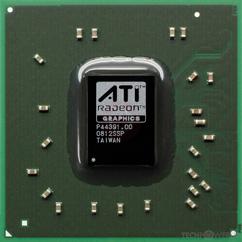
RV620

SIC66SIC66
Die Shot
ATI's RV620 GPU uses the TeraScale architecture and is made using a 55 nm production process at TSMC. With a die size of 67 mm² and a transistor count of 181 million it is a very small chip. RV620 supports DirectX 10.1 (Feature Level 10_1). For GPU compute applications, OpenCL version N/A can be used. It features 40 shading units, 4 texture mapping units and 4 ROPs.
Further reading:
R600 Series Instruction Set Architecture 
Graphics Processor
- Released
- Dec 10th, 2007
- GPU Name
- RV620
- Mobile Variant
- M82 / M84
- Codename
- Koopa
- Architecture
- TeraScale
- Foundry
- TSMC
- Process Size
- 55 nm
- Transistors
- 181 million
- Density
- 2.7M / mm²
- Die Size
- 67 mm²
- Package
- FCBGA-632
Graphics Features
- DirectX
- 10.1 (10_1)
- OpenGL
- 3.3
- OpenCL
- N/A
- Vulkan
- N/A
- Shader Model
- 4.1
- WDDM
- 1.1
- Compute
- GFX3
- DCE
- 3.0
- UVD
- 1.0
Render Config
- Shading Units
- 40
- TMUs
- 4
- ROPs
- 4
- Compute Units
- 2
- Vertex Cache
- 32 KB
- Texture Cache
- 32 KB
- Tex L1 Cache
- 32 KB per 4 SPs
- L2 Cache
- 64 KB
- Max. TDP
- 50 W
All TeraScale GPUs
- ATI M72
- ATI M74
- ATI M76
- ATI M82
- ATI M84
- ATI M86
- ATI M88
- ATI M92
- AMD M93
- ATI M93
- ATI M96
- ATI M97
- ATI M98
- ATI R600
- ATI R680
- ATI R700
- ATI RS780
- ATI RS880
- ATI RV610
- ATI RV620
- ATI RV630
- ATI RV635
- ATI RV670
- AMD RV670
- ATI RV710
- AMD RV711
- ATI RV711
- ATI RV730
- ATI RV740
- ATI RV770
- AMD RV770
- ATI RV790
- ATI RX881
- ATI Theater 650 PRO
- ATI Xenos Corona
- ATI Xenos Falcon
- ATI Xenos Jasper
- ATI Xenos Vejle
- ATI Xenos Xenon
ATI GPU Architecture History
Graphics cards using the ATI RV620 GPU
| Name | Chip | Memory | Shaders | TMUs | ROPs | GPU Clock | Memory Clock |
|---|---|---|---|---|---|---|---|
| RV620 LE | 256 MB | 40 | 4 | 4 | 600 MHz | 500 MHz | |
| RV620 PRO | 256 MB | 40 | 4 | 4 | 800 MHz | 950 MHz | |
| RV620 LE | 512 MB | 40 | 4 | 4 | 600 MHz | 400 MHz | |
| RV620 LE | 512 MB | 40 | 4 | 4 | 600 MHz | 500 MHz | |
| 256 MB | 40 | 4 | 4 | 500 MHz | 500 MHz | ||
| 256 MB | 40 | 4 | 4 | 500 MHz | 500 MHz | ||
| RV620 GL | 256 MB | 40 | 4 | 4 | 800 MHz | 950 MHz | |
| RV620 PRO | 256 MB | 40 | 4 | 4 | 400 MHz | 400 MHz | |
| 256 MB | 40 | 4 | 4 | 500 MHz | 500 MHz | ||
| RC620 PRO | 256 MB | 40 | 4 | 4 | 400 MHz | 400 MHz | |
| RV620 LE | 512 MB | 40 | 4 | 4 | 594 MHz | 396 MHz | |
| RV620 PRO | 512 MB | 40 | 4 | 4 | 594 MHz | 396 MHz | |
| RV620 PRO | 512 MB | 40 | 4 | 4 | 796 MHz | 495 MHz | |
| RV620 LE | 512 MB | 40 | 4 | 4 | 600 MHz | 500 MHz |


RV620 GPU Notes
| Mobile Variant: M82 / M84 Codename: Koopa Graphics/Compute: GFX3 Display Core Engine: 3.0 Unified Video Decoder: 1.0 |
Apr 24th, 2024 18:13 EDT
change timezone
Latest GPU Drivers
New Forum Posts
- Will a RTX 4070 TI super bottleneck a Ryzen 9 7950X3D? (56)
- Is there a technical reason that Windows 11 doesn't have built into it battery charge limitation? (41)
- Best SSD for system drive (75)
- How are MX330 and İ5 1135G7 ? (9)
- GTX 1070 Ti - TDP Issues - Always Power Throttling (1)
- 3DMARK "LEGENDARY" (189)
- TPU's Nostalgic Hardware Club (18462)
- Meta Horizon OS (14)
- im new to throttelstop and i think i messed it up by copying others any hints would be very much aprreciated (0)
- Is It The 1080 TI The Best GPU Ever? (214)
Popular Reviews
- Fractal Design Terra Review
- Thermalright Phantom Spirit 120 EVO Review
- Corsair 2000D Airflow Review
- Minisforum EliteMini UM780 XTX (AMD Ryzen 7 7840HS) Review
- ASUS GeForce RTX 4090 STRIX OC Review
- NVIDIA GeForce RTX 4090 Founders Edition Review - Impressive Performance
- ASUS GeForce RTX 4090 Matrix Platinum Review - The RTX 4090 Ti
- MSI GeForce RTX 4090 Gaming X Trio Review
- MSI GeForce RTX 4090 Suprim X Review
- Gigabyte GeForce RTX 4090 Gaming OC Review
Controversial News Posts
- Sony PlayStation 5 Pro Specifications Confirmed, Console Arrives Before Holidays (116)
- NVIDIA Points Intel Raptor Lake CPU Users to Get Help from Intel Amid System Instability Issues (106)
- AMD "Strix Halo" Zen 5 Mobile Processor Pictured: Chiplet-based, Uses 256-bit LPDDR5X (101)
- US Government Wants Nuclear Plants to Offload AI Data Center Expansion (98)
- Windows 10 Security Updates to Cost $61 After 2025, $427 by 2028 (84)
- Developers of Outpost Infinity Siege Recommend Underclocking i9-13900K and i9-14900K for Stability on Machines with RTX 4090 (84)
- TechPowerUp Hiring: Reviewers Wanted for Motherboards, Laptops, Gaming Handhelds and Prebuilt Desktops (78)
- Intel Realizes the Only Way to Save x86 is to Democratize it, Reopens x86 IP Licensing (70)