Report an Error


ATI RV635
RV635

RV635 PRO

Die Shot
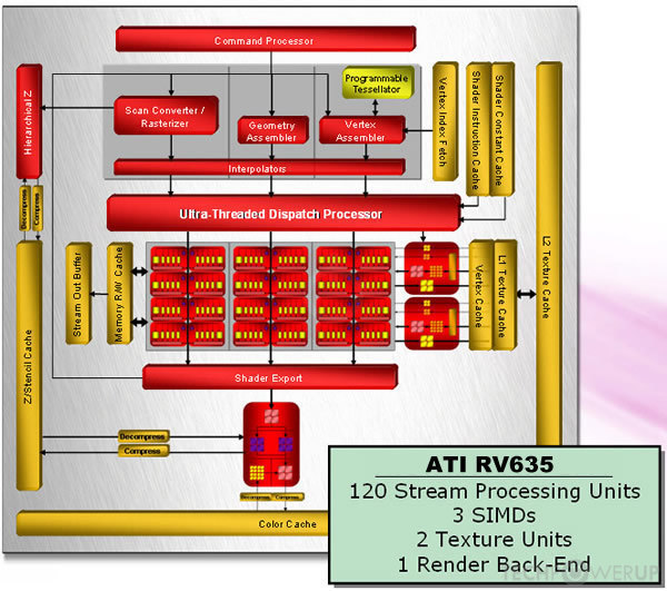
Block Diagram
ATI's RV635 GPU uses the TeraScale architecture and is made using a 55 nm production process at TSMC. With a die size of 135 mm² and a transistor count of 378 million it is a small chip. RV635 supports DirectX 10.1 (Feature Level 10_1). For GPU compute applications, OpenCL version N/A can be used. It features 120 shading units, 8 texture mapping units and 4 ROPs.
Further reading:
R600 Series Instruction Set Architecture 
Graphics Processor
- Released
- Jun 28th, 2007
- GPU Name
- RV635
- Mobile Variant
- M86
- Codename
- Wario
- Architecture
- TeraScale
- Foundry
- TSMC
- Process Size
- 55 nm
- Transistors
- 378 million
- Density
- 2.8M / mm²
- Die Size
- 135 mm²
- Package
- FCBGA-880
Graphics Features
- DirectX
- 10.1 (10_1)
- OpenGL
- 3.3
- OpenCL
- N/A
- Vulkan
- N/A
- Shader Model
- 4.1
- WDDM
- 1.1
- Compute
- GFX3
- DCE
- 3.0
- UVD
- 1.0
Render Config
- Shading Units
- 120
- TMUs
- 8
- ROPs
- 4
- Compute Units
- 3
- Z-Stencil
- 8
- Vertex Cache
- 32 KB
- Texture Cache
- 32 KB
- Tex L1 Cache
- 32 KB per 4 SPs
- L2 Cache
- 128 KB
- Max. TDP
- 65 W
All TeraScale GPUs
- ATI M72
- ATI M74
- ATI M76
- ATI M82
- ATI M84
- ATI M86
- ATI M88
- ATI M92
- AMD M93
- ATI M93
- ATI M96
- ATI M97
- ATI M98
- ATI R600
- ATI R680
- ATI R700
- ATI RS780
- ATI RS880
- ATI RV610
- ATI RV620
- ATI RV630
- ATI RV635
- ATI RV670
- AMD RV670
- ATI RV710
- AMD RV711
- ATI RV711
- ATI RV730
- ATI RV740
- ATI RV770
- AMD RV770
- ATI RV790
- ATI RX881
- ATI Theater 650 PRO
- ATI Xenos Corona
- ATI Xenos Falcon
- ATI Xenos Jasper
- ATI Xenos Vejle
- ATI Xenos Xenon
ATI GPU Architecture History
Graphics cards using the ATI RV635 GPU
| Name | Chip | Memory | Shaders | TMUs | ROPs | GPU Clock | Memory Clock |
|---|---|---|---|---|---|---|---|
| RV635 PRO | 256 MB | 120 | 8 | 4 | 725 MHz | 800 MHz | |
| RV635 PRO AGP | 512 MB | 120 | 8 | 4 | 725 MHz | 500 MHz | |
| RV635 PRO | 512 MB | 120 | 8 | 4 | 725 MHz | 600 MHz | |
| RV635 PRO | 512 MB | 120 | 8 | 4 | 722 MHz | 396 MHz | |
| RV635 PRO | 512 MB | 120 | 8 | 4 | 796 MHz | 693 MHz | |
| RV635 PRO | 512 MB | 120 | 8 | 4 | 796 MHz | 693 MHz | |
| RV635 PRO | 1024 MB | 120 | 8 | 4 | 796 MHz | 396 MHz | |
| 256 MB | 120 | 8 | 4 | 722 MHz | 405 MHz |


RV635 GPU Notes
| Mobile Variant: M86 Codename: Wario Graphics/Compute: GFX3 Display Core Engine: 3.0 Unified Video Decoder: 1.0 |
Apr 25th, 2024 14:54 EDT
change timezone
Latest GPU Drivers
New Forum Posts
- What phone you use as your daily driver? And, a discussion of them. (1477)
- Will a RTX 4070 TI super bottleneck a Ryzen 9 7950X3D? (59)
- Alphacool CORE 1 CPU block - bulging with danger of splitting? (13)
- Black screen after muting (3)
- What are you playing? (20527)
- How to check flatness of CPUs and coolers - INK and OPTICAL INTERFERENCE methods (111)
- Ghetto Mods (4321)
- Random blue screen from winload.efi error (0xc000000e) (2)
- Meta Horizon OS (20)
- WCG Daily Numbers (12497)
Popular Reviews
- Fractal Design Terra Review
- Thermalright Phantom Spirit 120 EVO Review
- Corsair 2000D Airflow Review
- Minisforum EliteMini UM780 XTX (AMD Ryzen 7 7840HS) Review
- ASUS GeForce RTX 4090 STRIX OC Review
- NVIDIA GeForce RTX 4090 Founders Edition Review - Impressive Performance
- ASUS GeForce RTX 4090 Matrix Platinum Review - The RTX 4090 Ti
- MSI GeForce RTX 4090 Suprim X Review
- MSI GeForce RTX 4090 Gaming X Trio Review
- Gigabyte GeForce RTX 4090 Gaming OC Review
Controversial News Posts
- Sony PlayStation 5 Pro Specifications Confirmed, Console Arrives Before Holidays (116)
- NVIDIA Points Intel Raptor Lake CPU Users to Get Help from Intel Amid System Instability Issues (106)
- Windows 11 Now Officially Adware as Microsoft Embeds Ads in the Start Menu (102)
- AMD "Strix Halo" Zen 5 Mobile Processor Pictured: Chiplet-based, Uses 256-bit LPDDR5X (101)
- US Government Wants Nuclear Plants to Offload AI Data Center Expansion (98)
- AMD's RDNA 4 GPUs Could Stick with 18 Gbps GDDR6 Memory (85)
- Developers of Outpost Infinity Siege Recommend Underclocking i9-13900K and i9-14900K for Stability on Machines with RTX 4090 (85)
- Windows 10 Security Updates to Cost $61 After 2025, $427 by 2028 (84)