Report an Error


ATI RV770
RV770
RV770 XT Mac

SIC66SIC66
Die Shot
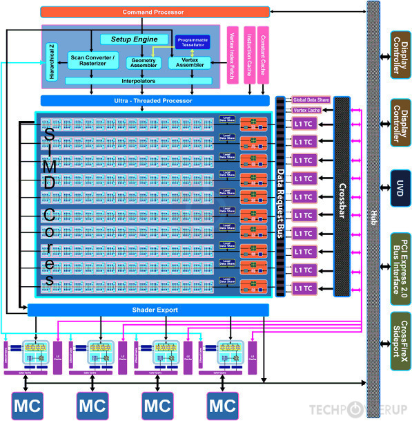
Block Diagram
ATI's RV770 GPU uses the TeraScale architecture and is made using a 55 nm production process at TSMC. With a die size of 256 mm² and a transistor count of 956 million it is a medium-sized chip. RV770 supports DirectX 10.1 (Feature Level 10_1). For GPU compute applications, OpenCL version 1.1 can be used. It features 800 shading units, 40 texture mapping units and 16 ROPs.
Further reading:
R700 Series Instruction Set Architecture 
Graphics Processor
- Released
- Jun 25th, 2008
- GPU Name
- RV770
- Mobile Variant
- M98
- Codename
- Wekiva
- Architecture
- TeraScale
- Foundry
- TSMC
- Process Size
- 55 nm
- Transistors
- 956 million
- Density
- 3.7M / mm²
- Die Size
- 256 mm²
- Package
- HFCBGA-1492
Graphics Features
- DirectX
- 10.1 (10_1)
- OpenGL
- 3.3
- OpenCL
- 1.1
- Vulkan
- N/A
- Shader Model
- 4.1
- WDDM
- 1.1
- Compute
- GFX3
- DCE
- 3.1
- UVD
- 2.0
Render Config
- Shading Units
- 800
- TMUs
- 40
- ROPs
- 16
- Compute Units
- 10
- Z-Stencil
- 64
- L1 Cache
- 16 KB per CU
- L2 Cache
- 256 KB
- Max. TDP
- 151 W
All TeraScale GPUs
- ATI M72
- ATI M74
- ATI M76
- ATI M82
- ATI M84
- ATI M86
- ATI M88
- ATI M92
- AMD M93
- ATI M93
- ATI M96
- ATI M97
- ATI M98
- ATI R600
- ATI R680
- ATI R700
- ATI RS780
- ATI RS880
- ATI RV610
- ATI RV620
- ATI RV630
- ATI RV635
- ATI RV670
- AMD RV670
- ATI RV710
- AMD RV711
- ATI RV711
- ATI RV730
- ATI RV740
- ATI RV770
- AMD RV770
- ATI RV790
- ATI RX881
- ATI Theater 650 PRO
- ATI Xenos Corona
- ATI Xenos Falcon
- ATI Xenos Jasper
- ATI Xenos Vejle
- ATI Xenos Xenon
ATI GPU Architecture History
Graphics cards using the ATI RV770 GPU
| Name | Chip | Memory | Shaders | TMUs | ROPs | GPU Clock | Memory Clock |
|---|---|---|---|---|---|---|---|
| RV770 XT | 512 MB | 800 | 40 | 16 | 750 MHz | 900 MHz | |
| RV770 LE | 512 MB | 640 | 32 | 16 | 575 MHz | 900 MHz | |
| RV770 CE | 512 MB | 640 | 32 | 8 | 750 MHz | 900 MHz | |
| RV770 PRO | 512 MB | 800 | 40 | 16 | 625 MHz | 993 MHz | |
| RV770 XT | 1024 MB | 800 | 40 | 16 | 750 MHz | 850 MHz | |
| RV770 XT | 2 GB | 800 | 40 | 16 | 750 MHz | 900 MHz | |
| RV770 XT | 1024 MB | 800 | 40 | 16 | 750 MHz | 850 MHz | |
| RV770 XT | 1024 MB | 800 | 40 | 8 | 625 MHz | 1050 MHz | |
| RV770 XT | 1024 MB | 800 | 40 | 8 | 750 MHz | 850 MHz | |
| RV770 CE | 512 MB | 640 | 32 | 8 | 625 MHz | 900 MHz | |
| RV770 XT Mac | 512 MB | 800 | 40 | 16 | 750 MHz | 850 MHz | |
| RV770 PRO | 512 MB | 640 | 32 | 16 | 575 MHz | 900 MHz |


RV770 GPU Notes
| Mobile Variant: M98 Codename: Wekiva Graphics/Compute: GFX3 Display Core Engine: 3.1 Unified Video Decoder: 2.0 |
Apr 19th, 2024 06:14 EDT
change timezone
Latest GPU Drivers
New Forum Posts
- Linus watercools (24)
- Should the CDPR make the Fallout 5 instead? (27)
- I7-8750H + GTX 1050ti Laptop drops performance periodically (0)
- Gelid Offering Odd Inconsistencies - WTF? (0)
- Roccat Kone AIMO has developed a double left click, when I click it once. Any fix out there? (28)
- First computer build for my son (3)
- FFMPEG commands for advanced enhanced image & video editing & conversion? (0)
- Do you use Linux? (230)
- Unlocked Realtek HD Audio Drivers for Windows 11 (Dolby Digital Live/DTS Interactive) (154)
- Ghetto Mods (4318)
Popular Reviews
- Horizon Forbidden West Performance Benchmark Review - 30 GPUs Tested
- PowerColor Radeon RX 7900 GRE Hellhound Review
- Fractal Design Terra Review
- Corsair 2000D Airflow Review
- Thermalright Phantom Spirit 120 EVO Review
- Minisforum EliteMini UM780 XTX (AMD Ryzen 7 7840HS) Review
- Creative Pebble X Plus Review
- FiiO KB3 HiFi Mechanical Keyboard Review - Integrated DAC/Amp!
- ASUS GeForce RTX 4090 STRIX OC Review
- NVIDIA GeForce RTX 4090 Founders Edition Review - Impressive Performance
Controversial News Posts
- Sony PlayStation 5 Pro Specifications Confirmed, Console Arrives Before Holidays (110)
- NVIDIA Points Intel Raptor Lake CPU Users to Get Help from Intel Amid System Instability Issues (102)
- US Government Wants Nuclear Plants to Offload AI Data Center Expansion (98)
- Windows 10 Security Updates to Cost $61 After 2025, $427 by 2028 (82)
- Developers of Outpost Infinity Siege Recommend Underclocking i9-13900K and i9-14900K for Stability on Machines with RTX 4090 (82)
- TechPowerUp Hiring: Reviewers Wanted for Motherboards, Laptops, Gaming Handhelds and Prebuilt Desktops (71)
- Intel Realizes the Only Way to Save x86 is to Democratize it, Reopens x86 IP Licensing (70)
- AMD Zen 5 Execution Engine Leaked, Features True 512-bit FPU (63)