Report an Error

ATI Xenos Vejle
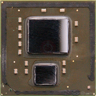
Xenos Vejle
ATI's Xenos Vejle GPU uses the TeraScale architecture and is made using a 45 nm production process at TSMC. With a die size of 168 mm² and a transistor count of 372 million it is a small chip. Xenos Vejle supports DirectX 9.0c (Feature Level 9_3). Modern GPU compute technologies are not available. It features 240 shading units, 16 texture mapping units and 8 ROPs.
Graphics Processor
- Released
- Jun 19th, 2010
- GPU Name
- Xenos Vejle
- Architecture
- TeraScale
- Foundry
- TSMC
- Process Size
- 45 nm
- Transistors
- 372 million
- Density
- 2.2M / mm²
- Die Size
- 168 mm²
Graphics Features
- DirectX
- 9.0c (9_3)
- OpenGL
- N/A
- OpenCL
- N/A
- Vulkan
- N/A
- Shader Model
- 3.0
Render Config
- Shading Units
- 240
- TMUs
- 16
- ROPs
- 8
- Compute Units
- 3
- Max. TDP
- 133 W
All TeraScale GPUs
- ATI M72
- ATI M74
- ATI M76
- ATI M82
- ATI M84
- ATI M86
- ATI M88
- ATI M92
- AMD M93
- ATI M93
- ATI M96
- ATI M97
- ATI M98
- ATI R600
- ATI R680
- ATI R700
- ATI RS780
- ATI RS880
- ATI RV610
- ATI RV620
- ATI RV630
- ATI RV635
- ATI RV670
- AMD RV670
- ATI RV710
- AMD RV711
- ATI RV711
- ATI RV730
- ATI RV740
- ATI RV770
- AMD RV770
- ATI RV790
- ATI RX881
- ATI Theater 650 PRO
- ATI Xenos Corona
- ATI Xenos Falcon
- ATI Xenos Jasper
- ATI Xenos Vejle
- ATI Xenos Xenon
ATI GPU Architecture History
Graphics cards using the ATI Xenos Vejle GPU
| Name | Chip | Memory | Shaders | TMUs | ROPs | GPU Clock | Memory Clock |
|---|---|---|---|---|---|---|---|
| Crayola 6 | 512 MB | 240 | 16 | 8 | 500 MHz | 700 MHz |

Xenos Vejle GPU Notes
| Transisters: CPU 140 million / GPU 232 million 48 floating-point vector processors for shader execution, divided in three dynamically scheduled SIMD groups of 16 processors each. Unified shading architecture (each pipeline is capable of running either pixel or vertex shaders) 10 FP ops per vector processor per cycle (5 fused multiply-add) Peak vertex count: 6.0 GVertices/s ((48 shader vector processors × 2 ops per cycle × 500 MHz) / 8 vector ops per vertex) for simple transformed and lit polygons Peak polygon count: 500 million triangles per second Peak shader operations: 96.0 billion shader operations/s (3 shader pipelines × 16 processors × 4 ALUs × 500 MHz) Floating Point Operations: 240.0 GFLOPS (3 shader pipelines × 16 processors × 500 MHz) MEMEXPORT shader function 16 texture filtering units 16 texture addressing units 16 filtered samples per clock Peak texel fillrate: 8.0 GTexel/s (16 textures × 500 MHz) 16 unfiltered texture samples per clock (16 texture addressing units) 8 Render Output units / pixel rendering pipelines Peak pixel fillrate: 4.0 GPixel/s without MSAA (8 ROPs × 500 MHz) Peak Z sample rate: 8.0 GSamples/s (2 Z samples × 8 ROPs × 500 MHz) 32.0 GSamples/s using 4X anti aliasing (2 Z samples × 8 ROPs × 4X AA × 500 MHz) Peak anti-aliasing sample rate: 16.0 GSamples/s (4 AA samples × 8 ROPs × 500 MHz) Peak Dot product operations: 24 billion per second Support for a superset of DirectX Xbox 360 10 MiB daughter embedded DRAM (at 256GB/s) framebuffer on NEC designed eDRAM die includes additional logic 105 million transistors (192 parallel pixel processors) for color, alpha compositing, Z/stencil buffering, and anti-aliasing called “Intelligent Memory”, giving developers 4-sample anti-aliasing at very little performance cost. |
Apr 23rd, 2024 22:13 EDT
change timezone
Latest GPU Drivers
New Forum Posts
- CPB Enabled Boot Loop (10)
- Upgrade Build (106)
- Official Board Game Discussion (9)
- TPU's Nostalgic Hardware Club (18461)
- The TPU UK Clubhouse (24771)
- Sexy Mechanical Keyboard Thread (485)
- Realtek Modded Audio Driver for Windows 10/11 - Only for HDAUDIO (5688)
- What's your latest tech purchase? (20319)
- Post your Cinebench 2024 score (449)
- need help with motherboard/ ram compability certainty (14)
Popular Reviews
- Fractal Design Terra Review
- Corsair 2000D Airflow Review
- Thermalright Phantom Spirit 120 EVO Review
- Minisforum EliteMini UM780 XTX (AMD Ryzen 7 7840HS) Review
- ASUS GeForce RTX 4090 STRIX OC Review
- NVIDIA GeForce RTX 4090 Founders Edition Review - Impressive Performance
- ASUS GeForce RTX 4090 Matrix Platinum Review - The RTX 4090 Ti
- MSI GeForce RTX 4090 Suprim X Review
- MSI GeForce RTX 4090 Gaming X Trio Review
- Gigabyte GeForce RTX 4090 Gaming OC Review
Controversial News Posts
- Sony PlayStation 5 Pro Specifications Confirmed, Console Arrives Before Holidays (116)
- NVIDIA Points Intel Raptor Lake CPU Users to Get Help from Intel Amid System Instability Issues (106)
- AMD "Strix Halo" Zen 5 Mobile Processor Pictured: Chiplet-based, Uses 256-bit LPDDR5X (101)
- US Government Wants Nuclear Plants to Offload AI Data Center Expansion (98)
- Windows 10 Security Updates to Cost $61 After 2025, $427 by 2028 (84)
- Developers of Outpost Infinity Siege Recommend Underclocking i9-13900K and i9-14900K for Stability on Machines with RTX 4090 (84)
- TechPowerUp Hiring: Reviewers Wanted for Motherboards, Laptops, Gaming Handhelds and Prebuilt Desktops (74)
- Intel Realizes the Only Way to Save x86 is to Democratize it, Reopens x86 IP Licensing (70)