Report an Error


ATI Hemlock

Hemlock
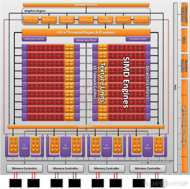
Block Diagram
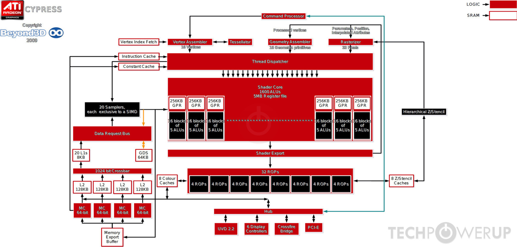
Block Diagram 2

Setup
ATI's Hemlock GPU uses the TeraScale 2 architecture and is made using a 40 nm production process at TSMC. With a die size of 334 mm² and a transistor count of 2,154 million it is a large chip. Hemlock supports DirectX 11.2 (Feature Level 11_0). For GPU compute applications, OpenCL version 1.2 can be used. It features 1600 shading units, 80 texture mapping units and 32 ROPs.
Further reading:
Evergreen Series Instruction Set Architecture 
Graphics Processor
- Released
- Nov 18th, 2009
- GPU Name
- Hemlock
- Desktop Variant
- Cypress
- Mobile Variant
- Lexington
- Generation
- Evergreen
- Architecture
- TeraScale 2
- Foundry
- TSMC
- Process Size
- 40 nm
- Transistors
- 2,154 million
- Density
- 6.4M / mm²
- Die Size
- 334 mm²
Graphics Features
- DirectX
- 11.2 (11_0)
- OpenGL
- 4.4
- OpenCL
- 1.2
- Vulkan
- N/A
- Shader Model
- 5.0
- WDDM
- 1.3
- Compute
- GFX4
- DCE
- 4.0
- UVD
- 2.3
Render Config
- Shading Units
- 1600
- TMUs
- 80
- ROPs
- 32
- Compute Units
- 20
- Z-Stencil
- 40
- L1 Cache
- 8 KB per CU
- L2 Cache
- 512 KB
- Max. TDP
- 302 W
All TeraScale 2 GPUs
- AMD Barts
- AMD Blackcomb
- ATI Broadway
- AMD Broadway
- AMD Caicos
- AMD Capilano
- ATI Cedar
- AMD Cedar
- ATI Cypress
- AMD Cypress
- AMD Granville
- ATI Hemlock
- AMD Juniper
- ATI Juniper
- AMD Latte
- AMD Lexington
- AMD Loveland
- ATI Madison
- AMD Onega
- ATI Park
- AMD Park
- ATI Pinewood
- AMD Pinewood
- ATI Redwood
- AMD Redwood
- AMD Robson
- AMD Seymour
- AMD Sumo
- AMD SuperSumo
- AMD Thames
- AMD Turks
- ATI Turks
- AMD Whistler
ATI GPU Architecture History
Graphics cards using the ATI Hemlock GPU
| Name | Chip | Memory | Shaders | TMUs | ROPs | GPU Clock | Memory Clock |
|---|---|---|---|---|---|---|---|
| Hemlock XT | 1024 MB | 1600 | 80 | 32 | 725 MHz | 1000 MHz | |
| Hemlock PRO | 1024 MB | 1440 | 72 | 32 | 725 MHz | 1000 MHz |


Hemlock GPU Notes
| Generation: Evergreen Desktop Variant: Cypress Mobile Variant: Lexington Graphics/Compute: GFX4 Display Core Engine: 4.0 Unified Video Decoder: 2.3 |
Apr 24th, 2024 08:05 EDT
change timezone
Latest GPU Drivers
New Forum Posts
- EK seems to be having major issues (32)
- Looking to build another system (0)
- Core i5-6300U (10)
- What phone you use as your daily driver? And, a discussion of them. (1460)
- What's your latest tech purchase? (20332)
- Which one to choose from these 3 laptops offer? (21)
- Blender 3.3.0 Benchmark (11)
- Will a RTX 4070 TI super bottleneck a Ryzen 9 7950X3D? (52)
- The TPU UK Clubhouse (24778)
- My computer setup - Request for opinions (14)
Popular Reviews
- Fractal Design Terra Review
- Corsair 2000D Airflow Review
- Thermalright Phantom Spirit 120 EVO Review
- Minisforum EliteMini UM780 XTX (AMD Ryzen 7 7840HS) Review
- ASUS GeForce RTX 4090 STRIX OC Review
- NVIDIA GeForce RTX 4090 Founders Edition Review - Impressive Performance
- ASUS GeForce RTX 4090 Matrix Platinum Review - The RTX 4090 Ti
- MSI GeForce RTX 4090 Suprim X Review
- MSI GeForce RTX 4090 Gaming X Trio Review
- Gigabyte GeForce RTX 4090 Gaming OC Review
Controversial News Posts
- Sony PlayStation 5 Pro Specifications Confirmed, Console Arrives Before Holidays (116)
- NVIDIA Points Intel Raptor Lake CPU Users to Get Help from Intel Amid System Instability Issues (106)
- AMD "Strix Halo" Zen 5 Mobile Processor Pictured: Chiplet-based, Uses 256-bit LPDDR5X (101)
- US Government Wants Nuclear Plants to Offload AI Data Center Expansion (98)
- Windows 10 Security Updates to Cost $61 After 2025, $427 by 2028 (84)
- Developers of Outpost Infinity Siege Recommend Underclocking i9-13900K and i9-14900K for Stability on Machines with RTX 4090 (84)
- TechPowerUp Hiring: Reviewers Wanted for Motherboards, Laptops, Gaming Handhelds and Prebuilt Desktops (77)
- Intel Realizes the Only Way to Save x86 is to Democratize it, Reopens x86 IP Licensing (70)