Report an Error


AMD Ellesmere

Ellesmere

Ellesmere PRO
Polaris 10 XT
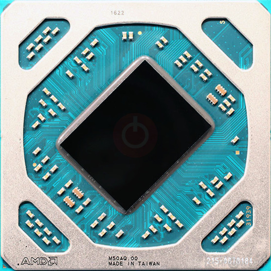
Fritzchens Fritz
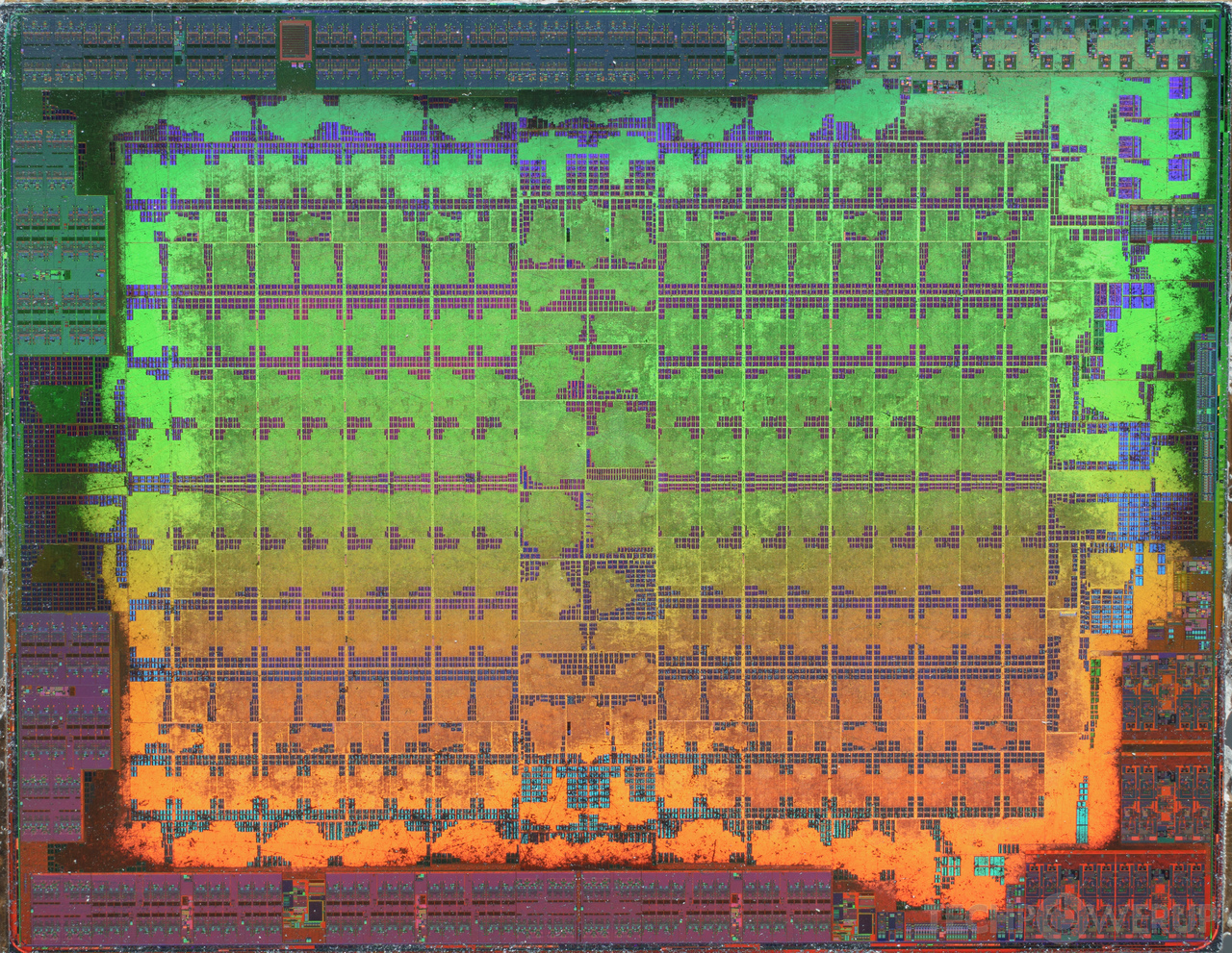
Die Shot

Block Diagram
AMD's Ellesmere GPU uses the GCN 4.0 architecture and is made using a 14 nm production process at GlobalFoundries. With a die size of 232 mm² and a transistor count of 5,700 million it is a medium-sized chip. Ellesmere supports DirectX 12 (Feature Level 12_0). For GPU compute applications, OpenCL version 2.1 can be used. It features 2304 shading units, 144 texture mapping units and 32 ROPs.
Further reading:
Polaris Architecture Whitepaper 
Graphics Processor
- Released
- Jun 29th, 2016
- GPU Name
- Ellesmere
- Codename
- Polaris 10/20/30
- Generation
- Arctic Islands
- Architecture
- GCN 4.0
- Foundry
- GlobalFoundries
- Process Size
- 14 nm
- Transistors
- 5,700 million
- Density
- 24.6M / mm²
- Die Size
- 232 mm²
- Package
- BGA-1401
Graphics Features
- DirectX
- 12 (12_0)
- OpenGL
- 4.6
- OpenCL
- 2.1
- Vulkan
- 1.3
- Shader Model
- 6.7
- WDDM
- 3.1
- Compute
- GFX8 (gfx803)
- DCE
- 11.2
- UVD
- 6.3
- VCE
- 3.4
- SDMA
- 3.0.0
- CLRX
- GCN 1.2.0
Render Config
- Shading Units
- 2304
- TMUs
- 144
- ROPs
- 32
- Compute Units
- 36
- ACEs
- 4
- HWSs
- 2
- SEs
- 4
- L1 Cache
- 16 KB per CU
- L2 Cache
- 2048 KB
- Max. TDP
- 250 W
All GCN 4.0 GPUs
AMD GPU Architecture History
- 2023 CDNA 3.0
- 2022-2024 RDNA 3.0
- 2021 CDNA 2.0
- 2020 CDNA 1.0
- 2020-2023 RDNA 2.0
- 2019-2020 RDNA 1.0
- 2018-2022 GCN 5.1
- 2017-2020 GCN 5.0
- 2016-2020 GCN 4.0
- 2014-2019 GCN 3.0
- 2013-2017 GCN 2.0
- 2011-2020 GCN 1.0
- 2010-2013 TeraScale 3
- 2009-2015 TeraScale 2
- 2005-2013 TeraScale
- 2005-2007 Ultra-Threaded SE
Graphics cards using the AMD Ellesmere GPU
| Name | Chip | Memory | Shaders | TMUs | ROPs | Base Clock | Boost Clock | Memory Clock |
|---|---|---|---|---|---|---|---|---|
| Polaris 10 XT | 8 GB | 2304 | 144 | 32 | 1120 MHz | 1266 MHz | 2000 MHz | |
| Polaris 10 PRO | 4 GB | 2048 | 128 | 32 | 926 MHz | 1206 MHz | 1650 MHz | |
| Polaris 10 XT GL | 8 GB | 2304 | 144 | 32 | 1188 MHz | 1243 MHz | 1750 MHz | |
| Polaris 10 PRO GL | 8 GB | 1792 | 112 | 32 | 713 MHz | 1086 MHz | 1250 MHz | |
| Polaris 10 E9550 | 8 GB | 2304 | 144 | 32 | 1120 MHz | 1244 MHz | 1250 MHz | |
| Polaris 10 PROD | 4 GB | 1792 | 112 | 32 | 926 MHz | 1206 MHz | 1650 MHz | |
| Ellesmere XT | 8 GB | 2304 | 144 | 32 | 1120 MHz | 1233 MHz | 1750 MHz | |
| Ellesmere Gemini GL | 16 GB | 2304 | 144 | 32 | 1243 MHz | 1750 MHz | ||
| Ellesmere XTA | 8 GB | 2304 | 144 | 32 | 1100 MHz | 1200 MHz | 1695 MHz | |
| Ellesmere XLA | 4 GB | 2048 | 128 | 32 | 1096 MHz | 1695 MHz | ||
| Ellesmere PROA | 4 GB | 1792 | 112 | 32 | 1000 MHz | 1105 MHz | 1695 MHz | |
| Ellesmere XT | 8 GB | 2304 | 144 | 32 | 1188 MHz | 1243 MHz | 1750 MHz | |
| Ellesmere Gemini GL | 16 GB | 2304 | 144 | 32 | 1188 MHz | 1243 MHz | 1750 MHz | |
| Ellesmere PRO | 8 GB | 2048 | 128 | 32 | 926 MHz | 1206 MHz | 1650 MHz | |
| Ellesmere PRO | 8 GB | 2048 | 128 | 32 | 926 MHz | 1074 MHz | 1750 MHz | |
| Ellesmere XT | 8 GB | 2304 | 144 | 32 | 1000 MHz | 1077 MHz | 2000 MHz | |
| Ellesmere XT GL | 8 GB | 2304 | 144 | 32 | 1188 MHz | 1243 MHz | 1250 MHz | |
| Polaris 10 XT | 8 GB | 2304 | 144 | 32 | 1120 MHz | 1266 MHz | 2000 MHz | |
| Polaris 10 LE1 | 4 GB | 1792 | 112 | 32 | 1074 MHz | 1226 MHz | 1750 MHz | |
| Ellesmere PROA | 4 GB | 1792 | 112 | 32 | 1000 MHz | 1105 MHz | 1695 MHz | |
| Ellesmere XLA | 4 GB | 2048 | 128 | 32 | 1096 MHz | 1695 MHz | ||
| Ellesmere XTA | 8 GB | 2304 | 144 | 32 | 1100 MHz | 1200 MHz | 1710 MHz | |
| Ellesmere XT GL | 8 GB | 2304 | 144 | 32 | 1188 MHz | 1243 MHz | 1250 MHz | |
| 8 GB | 2304 | 144 | 32 | 1120 MHz | 1237 MHz | 1750 MHz | ||
| 8 GB | 1792 | 112 | 32 | 713 MHz | 1089 MHz | 1250 MHz |


Ellesmere GPU Notes
| Generation: Arctic Islands Codename: Polaris 10/20/30 Old Codename: Cozumel / Hawaii Refresh Graphics/Compute: GFX8 (gfx803) Display Core Engine: 11.2 Unified Video Decoder: 6.3 Video Compression Engine: 3.4 System DMA: 3.0.0 CLRX: GCN 1.2.0 |
Apr 25th, 2024 14:13 EDT
change timezone
Latest GPU Drivers
New Forum Posts
- What phone you use as your daily driver? And, a discussion of them. (1474)
- Black screen after muting (2)
- What are you playing? (20527)
- How to check flatness of CPUs and coolers - INK and OPTICAL INTERFERENCE methods (111)
- Alphacool CORE 1 CPU block - bulging with danger of splitting? (11)
- Ghetto Mods (4321)
- Random blue screen from winload.efi error (0xc000000e) (2)
- Meta Horizon OS (20)
- WCG Daily Numbers (12497)
- Share your AIDA 64 cache and memory benchmark here (2917)
Popular Reviews
- Fractal Design Terra Review
- Thermalright Phantom Spirit 120 EVO Review
- Corsair 2000D Airflow Review
- Minisforum EliteMini UM780 XTX (AMD Ryzen 7 7840HS) Review
- ASUS GeForce RTX 4090 STRIX OC Review
- NVIDIA GeForce RTX 4090 Founders Edition Review - Impressive Performance
- ASUS GeForce RTX 4090 Matrix Platinum Review - The RTX 4090 Ti
- MSI GeForce RTX 4090 Suprim X Review
- MSI GeForce RTX 4090 Gaming X Trio Review
- Gigabyte GeForce RTX 4090 Gaming OC Review
Controversial News Posts
- Sony PlayStation 5 Pro Specifications Confirmed, Console Arrives Before Holidays (116)
- NVIDIA Points Intel Raptor Lake CPU Users to Get Help from Intel Amid System Instability Issues (106)
- AMD "Strix Halo" Zen 5 Mobile Processor Pictured: Chiplet-based, Uses 256-bit LPDDR5X (101)
- Windows 11 Now Officially Adware as Microsoft Embeds Ads in the Start Menu (99)
- US Government Wants Nuclear Plants to Offload AI Data Center Expansion (98)
- AMD's RDNA 4 GPUs Could Stick with 18 Gbps GDDR6 Memory (85)
- Developers of Outpost Infinity Siege Recommend Underclocking i9-13900K and i9-14900K for Stability on Machines with RTX 4090 (85)
- Windows 10 Security Updates to Cost $61 After 2025, $427 by 2028 (84)