Report an Error


NVIDIA GeForce 8500 GT
- Graphics Processor
- G86
- Cores
- 16
- TMUs
- 8
- ROPs
- 4
- Memory Size
- 256 MB
- Memory Type
- GDDR3
- Bus Width
- 128 bit

GPU
Recommended Gaming Resolutions:
- 640x480
- 1280x720
- 1366x768
The GeForce 8500 GT was a mid-range graphics card by NVIDIA, launched on April 17th, 2007. Built on the 80 nm process, and based on the G86 graphics processor, in its G86-300-A2 variant, the card supports DirectX 11.1. Even though it supports DirectX 11, the feature level is only 10_0, which can be problematic with many DirectX 11 & DirectX 12 titles. The G86 graphics processor is an average sized chip with a die area of 127 mm² and 210 million transistors. It features 16 shading units, 8 texture mapping units, and 4 ROPs. NVIDIA has paired 256 MB GDDR3 memory with the GeForce 8500 GT, which are connected using a 128-bit memory interface. The GPU is operating at a frequency of 459 MHz, memory is running at 400 MHz.
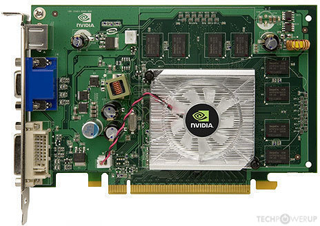
Being a single-slot card, the NVIDIA GeForce 8500 GT does not require any additional power connector, its power draw is rated at 30 W maximum. Display outputs include: 1x DVI, 1x VGA, 1x S-Video. GeForce 8500 GT is connected to the rest of the system using a PCI-Express 1.0 x16 interface. The card measures 229 mm in length, and features a single-slot cooling solution. Its price at launch was 129 US Dollars.
Being a single-slot card, the NVIDIA GeForce 8500 GT does not require any additional power connector, its power draw is rated at 30 W maximum. Display outputs include: 1x DVI, 1x VGA, 1x S-Video. GeForce 8500 GT is connected to the rest of the system using a PCI-Express 1.0 x16 interface. The card measures 229 mm in length, and features a single-slot cooling solution. Its price at launch was 129 US Dollars.
Graphics Processor
Graphics Card
- Release Date
- Apr 17th, 2007
- Generation
-
GeForce 8
(8500)
- Predecessor
- GeForce 7 PCIe
- Successor
- GeForce 9
- Production
- End-of-life
- Launch Price
- 129 USD
- Bus Interface
- PCIe 1.0 x16
- Reviews
- 33 in our database
Relative Performance
Based on TPU review data: "Performance Summary" at 1920x1080, 4K for 2080 Ti and faster.
Performance estimated based on architecture, shader count and clocks.
Clock Speeds
- GPU Clock
- 459 MHz
- Shader Clock
- 918 MHz
- Memory Clock
-
400 MHz
800 Mbps effective
Memory
- Memory Size
- 256 MB
- Memory Type
- GDDR3
- Memory Bus
- 128 bit
- Bandwidth
- 12.80 GB/s
Render Config
- Shading Units
- 16
- TMUs
- 8
- ROPs
- 4
- SM Count
- 2
- L2 Cache
- 32 KB
Theoretical Performance
- Pixel Rate
- 1.836 GPixel/s
- Texture Rate
- 3.672 GTexel/s
- FP32 (float)
- 29.38 GFLOPS
Board Design
- Slot Width
- Single-slot
- Length
- 229 mm
9 inches
- TDP
- 30 W
- Suggested PSU
- 200 W
- Outputs
- 1x DVI
1x VGA
1x S-Video
- Power Connectors
- None
- Board Number
- P403
Graphics Features
- DirectX
- 11.1 (10_0)
- OpenGL
- 3.3
- OpenCL
- 1.1
- Vulkan
- N/A
- CUDA
- 1.1
- Shader Model
- 4.0
Card Notes
| Memory Variant: 512 MB Memory Variant: 1024 MB |
G86 GPU Notes
| PureVideo HD: VP2 VDPAU: Feature Set A |
Retail boards based on this design (4)
| Name | GPU Clock | Memory Clock | Other Changes |
|---|---|---|---|
| 475 MHz | 475 MHz | DDR2 | |
| 600 MHz | 700 MHz | ||
| 600 MHz | 750 MHz | ||
| 700 MHz | 400 MHz | DDR2, 165 mm/6.5 inches |


Apr 19th, 2024 03:34 EDT
change timezone
Latest GPU Drivers
New Forum Posts
- First computer build for my son (2)
- Linus watercools (18)
- Unlocked Realtek HD Audio Drivers for Windows 11 (Dolby Digital Live/DTS Interactive) (154)
- Ghetto Mods (4318)
- Identify my GPU - RX 570 8GB (or what?) (3)
- FINAL FANTASY XIV: Dawntrail Official Benchmark (58)
- What's your latest tech purchase? (20283)
- Should the CDPR make the Fallout 5 instead? (23)
- Will a RTX 4070 TI super bottleneck a Ryzen 9 7950X3D? (36)
- DDR5 RAM Speeds and the future (45)
Popular Reviews
- Horizon Forbidden West Performance Benchmark Review - 30 GPUs Tested
- PowerColor Radeon RX 7900 GRE Hellhound Review
- Fractal Design Terra Review
- Corsair 2000D Airflow Review
- Minisforum EliteMini UM780 XTX (AMD Ryzen 7 7840HS) Review
- Thermalright Phantom Spirit 120 EVO Review
- Creative Pebble X Plus Review
- FiiO KB3 HiFi Mechanical Keyboard Review - Integrated DAC/Amp!
- ASUS GeForce RTX 4090 STRIX OC Review
- NVIDIA GeForce RTX 4090 Founders Edition Review - Impressive Performance
Controversial News Posts
- Sony PlayStation 5 Pro Specifications Confirmed, Console Arrives Before Holidays (110)
- NVIDIA Points Intel Raptor Lake CPU Users to Get Help from Intel Amid System Instability Issues (102)
- US Government Wants Nuclear Plants to Offload AI Data Center Expansion (98)
- Windows 10 Security Updates to Cost $61 After 2025, $427 by 2028 (82)
- Developers of Outpost Infinity Siege Recommend Underclocking i9-13900K and i9-14900K for Stability on Machines with RTX 4090 (82)
- TechPowerUp Hiring: Reviewers Wanted for Motherboards, Laptops, Gaming Handhelds and Prebuilt Desktops (71)
- Intel Realizes the Only Way to Save x86 is to Democratize it, Reopens x86 IP Licensing (70)
- AMD Zen 5 Execution Engine Leaked, Features True 512-bit FPU (63)