Report an Error


NVIDIA GeForce GT 330M
- Graphics Processor
- GT216
- Cores
- 48
- TMUs
- 16
- ROPs
- 8
- Memory Size
- 1024 MB
- Memory Type
- GDDR3
- Bus Width
- 128 bit

GPU
Recommended Gaming Resolutions:
- 640x480
- 1280x720
- 1366x768
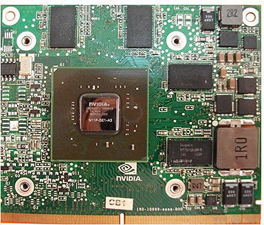
The GeForce GT 330M was a mobile graphics chip by NVIDIA, launched on January 10th, 2010. Built on the 40 nm process, and based on the GT216 graphics processor, in its N11P-GE1-A3 variant, the chip supports DirectX 11.1. Even though it supports DirectX 11, the feature level is only 10_1, which can be problematic with many DirectX 11 & DirectX 12 titles. The GT216 graphics processor is a relatively small chip with a die area of only 100 mm² and 486 million transistors. It features 48 shading units, 16 texture mapping units, and 8 ROPs. NVIDIA has paired 1,024 MB GDDR3 memory with the GeForce GT 330M, which are connected using a 128-bit memory interface. The GPU is operating at a frequency of 575 MHz, memory is running at 790 MHz.
Being a mxm module card, the NVIDIA GeForce GT 330M does not require any additional power connector, its power draw is rated at 23 W maximum. This device has no display connectivity, as it is not designed to have monitors connected to it. Rather it is intended for use in laptop/notebooks and will use the output of the host mobile device.
Being a mxm module card, the NVIDIA GeForce GT 330M does not require any additional power connector, its power draw is rated at 23 W maximum. This device has no display connectivity, as it is not designed to have monitors connected to it. Rather it is intended for use in laptop/notebooks and will use the output of the host mobile device.
Graphics Processor
Mobile Graphics
- Release Date
- Jan 10th, 2010
- Generation
- GeForce 300M
- Predecessor
- GeForce 200M
- Successor
- GeForce 400M
- Production
- End-of-life
- Bus Interface
- MXM-A (3.0)
- Reviews
- 2 in our database
Relative Performance
Based on TPU review data: "Performance Summary" at 1920x1080, 4K for 2080 Ti and faster.
Performance estimated based on architecture, shader count and clocks.
Clock Speeds
- GPU Clock
- 575 MHz
- Shader Clock
- 1265 MHz
- Memory Clock
-
790 MHz
1580 Mbps effective
Memory
- Memory Size
- 1024 MB
- Memory Type
- GDDR3
- Memory Bus
- 128 bit
- Bandwidth
- 25.28 GB/s
Render Config
- Shading Units
- 48
- TMUs
- 16
- ROPs
- 8
- SM Count
- 6
- L2 Cache
- 64 KB
Theoretical Performance
- Pixel Rate
- 4.600 GPixel/s
- Texture Rate
- 9.200 GTexel/s
- FP32 (float)
- 121.4 GFLOPS
Board Design
- Slot Width
- MXM Module
- TDP
- 23 W
- Outputs
- Portable Device Dependent
- Power Connectors
- None
- Board Number
- E696 SKU 89,
E696 SKU 189,
P681
Graphics Features
- DirectX
- 11.1 (10_1)
- OpenGL
- 3.3
- OpenCL
- 1.1
- Vulkan
- N/A
- CUDA
- 1.2
- Shader Model
- 4.1
GT216 GPU Notes
| PureVideo HD: VP4 VDPAU: Feature Set C |
Devices based on this design (1)
| Name | GPU Clock | Memory Clock | Other Changes |
|---|---|---|---|
| 500 MHz | 790 MHz |
Apr 25th, 2024 19:52 EDT
change timezone
Latest GPU Drivers
New Forum Posts
- Core PL1 + GPU PL1 + Ring EDP OTHER (10)
- Size on Disk Excessively Different than Size (8)
- Best SSD for system drive (80)
- Dell Workstation Owners Club (3055)
- Which new games will you be buying? (315)
- BSOD if I touch the pcache offset voltage in throttlestop (i9-13900hx lenovo pro 7i) (23)
- Alphacool CORE 1 CPU block - bulging with danger of splitting? (16)
- How to check flatness of CPUs and coolers - INK and OPTICAL INTERFERENCE methods (112)
- TPU's Nostalgic Hardware Club (18464)
- Post your Cinebench 2024 score (450)
Popular Reviews
- Fractal Design Terra Review
- Thermalright Phantom Spirit 120 EVO Review
- Corsair 2000D Airflow Review
- Minisforum EliteMini UM780 XTX (AMD Ryzen 7 7840HS) Review
- ASUS GeForce RTX 4090 STRIX OC Review
- NVIDIA GeForce RTX 4090 Founders Edition Review - Impressive Performance
- ASUS GeForce RTX 4090 Matrix Platinum Review - The RTX 4090 Ti
- MSI GeForce RTX 4090 Suprim X Review
- MSI GeForce RTX 4090 Gaming X Trio Review
- Gigabyte GeForce RTX 4090 Gaming OC Review
Controversial News Posts
- Sony PlayStation 5 Pro Specifications Confirmed, Console Arrives Before Holidays (117)
- Windows 11 Now Officially Adware as Microsoft Embeds Ads in the Start Menu (107)
- NVIDIA Points Intel Raptor Lake CPU Users to Get Help from Intel Amid System Instability Issues (106)
- AMD "Strix Halo" Zen 5 Mobile Processor Pictured: Chiplet-based, Uses 256-bit LPDDR5X (101)
- US Government Wants Nuclear Plants to Offload AI Data Center Expansion (98)
- AMD's RDNA 4 GPUs Could Stick with 18 Gbps GDDR6 Memory (88)
- Developers of Outpost Infinity Siege Recommend Underclocking i9-13900K and i9-14900K for Stability on Machines with RTX 4090 (85)
- Windows 10 Security Updates to Cost $61 After 2025, $427 by 2028 (84)