Report an Error


NVIDIA GeForce GT 640 OEM Rebrand
- Graphics Processor
- GF116
- Cores
- 144
- TMUs
- 24
- ROPs
- 24
- Memory Size
- 1536 MB
- Memory Type
- DDR3
- Bus Width
- 192 bit

GPU
Recommended Gaming Resolutions:
- 1280x720
- 1366x768
- 1600x900
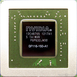
The GeForce GT 640 OEM Rebrand was a graphics card by NVIDIA, launched on April 24th, 2012. Built on the 40 nm process, and based on the GF116 graphics processor, in its GF116-150-A1 variant, the card supports DirectX 12. Even though it supports DirectX 12, the feature level is only 11_0, which can be problematic with newer DirectX 12 titles. The GF116 graphics processor is an average sized chip with a die area of 238 mm² and 1,170 million transistors. Unlike the fully unlocked GeForce GTX 550 Ti, which uses the same GPU but has all 192 shaders enabled, NVIDIA has disabled some shading units on the GeForce GT 640 OEM Rebrand to reach the product's target shader count. It features 144 shading units, 24 texture mapping units, and 24 ROPs. NVIDIA has paired 1,536 MB DDR3 memory with the GeForce GT 640 OEM Rebrand, which are connected using a 192-bit memory interface. The GPU is operating at a frequency of 720 MHz, memory is running at 800 MHz.
Being a single-slot card, the NVIDIA GeForce GT 640 OEM Rebrand does not require any additional power connector, its power draw is rated at 75 W maximum. Display outputs include: 2x DVI, 1x mini-HDMI 1.3a. GeForce GT 640 OEM Rebrand is connected to the rest of the system using a PCI-Express 2.0 x16 interface. The card measures 145 mm in length, and features a single-slot cooling solution.
Being a single-slot card, the NVIDIA GeForce GT 640 OEM Rebrand does not require any additional power connector, its power draw is rated at 75 W maximum. Display outputs include: 2x DVI, 1x mini-HDMI 1.3a. GeForce GT 640 OEM Rebrand is connected to the rest of the system using a PCI-Express 2.0 x16 interface. The card measures 145 mm in length, and features a single-slot cooling solution.
Graphics Processor
Graphics Card
- Release Date
- Apr 24th, 2012
- Generation
- GeForce 600
- Predecessor
- GeForce 500
- Successor
- GeForce 700
- Production
- End-of-life
- Bus Interface
- PCIe 2.0 x16
Relative Performance
Based on TPU review data: "Performance Summary" at 1920x1080, 4K for 2080 Ti and faster.
Performance estimated based on architecture, shader count and clocks.
Clock Speeds
- GPU Clock
- 720 MHz
- Shader Clock
- 1440 MHz
- Memory Clock
-
800 MHz
1600 Mbps effective
Memory
- Memory Size
- 1536 MB
- Memory Type
- DDR3
- Memory Bus
- 192 bit
- Bandwidth
- 38.40 GB/s
Render Config
- Shading Units
- 144
- TMUs
- 24
- ROPs
- 24
- SM Count
- 3
- L1 Cache
- 64 KB (per SM)
- L2 Cache
- 384 KB
Theoretical Performance
- Pixel Rate
- 4.320 GPixel/s
- Texture Rate
- 17.28 GTexel/s
- FP32 (float)
- 414.7 GFLOPS
- FP64 (double)
- 34.56 GFLOPS (1:12)
Board Design
- Slot Width
- Single-slot
- Length
- 145 mm
5.7 inches
- TDP
- 75 W
- Suggested PSU
- 250 W
- Outputs
- 2x DVI
1x mini-HDMI 1.3a
- Power Connectors
- None
- Board Number
- P1062 SKU 16,
P1062 SKU 17,
P1062 SKU 18
Graphics Features
- DirectX
- 12 (11_0)
- OpenGL
- 4.6
- OpenCL
- 1.1
- Vulkan
- N/A
- CUDA
- 2.1
- Shader Model
- 5.1
GF116 GPU Notes
| PureVideo HD: VP4 VDPAU: Feature Set C |
Retail boards based on this design (1)
| Name | GPU Clock | Memory Clock | Other Changes |
|---|---|---|---|
| 720 MHz | 800 MHz | 3 GB, 1x DVI 1x HDMI 1x DisplayPort |

Apr 25th, 2024 19:55 EDT
change timezone
Latest GPU Drivers
New Forum Posts
- Core PL1 + GPU PL1 + Ring EDP OTHER (10)
- Size on Disk Excessively Different than Size (8)
- Best SSD for system drive (80)
- Dell Workstation Owners Club (3055)
- Which new games will you be buying? (315)
- BSOD if I touch the pcache offset voltage in throttlestop (i9-13900hx lenovo pro 7i) (23)
- Alphacool CORE 1 CPU block - bulging with danger of splitting? (16)
- How to check flatness of CPUs and coolers - INK and OPTICAL INTERFERENCE methods (112)
- TPU's Nostalgic Hardware Club (18464)
- Post your Cinebench 2024 score (450)
Popular Reviews
- Fractal Design Terra Review
- Thermalright Phantom Spirit 120 EVO Review
- Corsair 2000D Airflow Review
- Minisforum EliteMini UM780 XTX (AMD Ryzen 7 7840HS) Review
- ASUS GeForce RTX 4090 STRIX OC Review
- NVIDIA GeForce RTX 4090 Founders Edition Review - Impressive Performance
- ASUS GeForce RTX 4090 Matrix Platinum Review - The RTX 4090 Ti
- MSI GeForce RTX 4090 Suprim X Review
- MSI GeForce RTX 4090 Gaming X Trio Review
- Gigabyte GeForce RTX 4090 Gaming OC Review
Controversial News Posts
- Sony PlayStation 5 Pro Specifications Confirmed, Console Arrives Before Holidays (117)
- Windows 11 Now Officially Adware as Microsoft Embeds Ads in the Start Menu (107)
- NVIDIA Points Intel Raptor Lake CPU Users to Get Help from Intel Amid System Instability Issues (106)
- AMD "Strix Halo" Zen 5 Mobile Processor Pictured: Chiplet-based, Uses 256-bit LPDDR5X (101)
- US Government Wants Nuclear Plants to Offload AI Data Center Expansion (98)
- AMD's RDNA 4 GPUs Could Stick with 18 Gbps GDDR6 Memory (88)
- Developers of Outpost Infinity Siege Recommend Underclocking i9-13900K and i9-14900K for Stability on Machines with RTX 4090 (85)
- Windows 10 Security Updates to Cost $61 After 2025, $427 by 2028 (84)